SlideShare a Scribd company logo
1 of 17
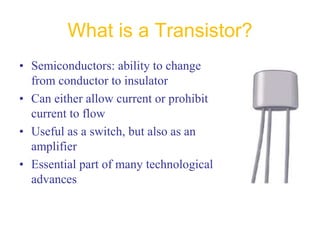
What is a Transistor?
• Semiconductors: ability to change
from conductor to insulator
• Can either allow current or prohibit
current to flow
• Useful as a switch, but also as an
amplifier
• Essential part of many technological
advances
A Brief History
• Guglielmo Marconi invents radio in 1895
• Problem: For long distance travel, signal must
be amplified
• Lee De Forest improves on Fleming’s original
vacuum tube to amplify signals
• Made use of third electrode
• Too bulky for most applications
The Transistor is Born
• Bell Labs (1947): Bardeen,
Brattain, and Shockley
• Originally made of germanium
• Current transistors made of
doped silicon
How Transistors Work
• Doping: adding small amounts of other
elements to create additional protons or
electrons
• P-Type: dopants lack a fourth valence electron
(Boron, Aluminum)
• N-Type: dopants have an additional (5th)
valence electron (Phosphorus, Arsenic)
• Importance: Current only flows from P to N
Diodes and Bias
• Diode: simple P-N junction.
• Forward Bias: allows current to
flow from P to N.
• Reverse Bias: no current allowed
to flow from N to P.
• Breakdown Voltage: sufficient N
to P voltage of a Zener Diode will
allow for current to flow in this
direction.
• 3 adjacent regions of doped
Si (each connected to a lead):
– Base. (thin layer,less doped).
– Collector.
– Emitter.
• 2 types of BJT:
– npn.
– pnp.
• Most common: npn (focus
on it).
Bipolar Junction Transistor (BJT)
npn bipolar junction transistor
pnp bipolar junction transistor
Developed by
Shockley (1949)
NPN Transistor
• 1 thin layer of p-type, sandwiched between 2 layers of n-type.
• N-type of emitter: more heavily doped than collector.
• With VC>VB>VE:
– Base-Emitter junction forward biased, Base-Collector reverse biased.
– Electrons diffuse from Emitter to Base (from n to p).
– There’s a depletion layer on the Base-Collector junction no flow of e-
allowed.
– BUT the Base is thin and Emitter region is n+ (heavily doped)  electrons
have enough momentum to cross the Base into the Collector.
– The small base current IB controls a large current IC
BJT NPN Transistor
• Current Gain:
– α is the fraction of electrons
that diffuse across the narrow
Base region
– 1- α is the fraction of electrons
that recombine with holes in
the Base region to create base
current
• The current Gain is expressed
in terms of the β (beta) of the
transistor (often called hfe by
manufacturers).
• β (beta) is Temperature and
Voltage dependent.
• It can vary a lot among
transistors (common values for
signal BJT: 20 - 200).
BJT characteristics











1
)
1
(
B
C
E
B
E
C
I
I
I
I
I
I
• Emitter is grounded.
• Base-Emitter starts to conduct with VBE=0.6V,IC flows and it’s IC=*IB.
• Increasing IB, VBE slowly increases to 0.7V but IC rises exponentially.
• As IC rises ,voltage drop across RC increases and VCE drops toward
ground. (transistor in saturation, no more linear relation between IC
and IB)
NPN Common Emitter circuit
Common Emitter characteristics
No current flows
Collector current
controlled by the
collector circuit.
(Switch behavior)
In full saturation
VCE=0.2V.
Collector current
proportional to
Base current
The avalanche
multiplication of
current through
collector junction
occurs: to be
avoided
Operation
Region
IB or VCE
Char.
BC and BE
Junctions
Mode
Cutoff IB = Very
small
Reverse &
Reverse
Open
Switch
Saturation VCE = Small Forward &
Forward
Closed
Switch
Active
Linear
VCE =
Moderate
Reverse &
Forward
Linear
Amplifier
Break-
down
VCE =
Large
Beyond
Limits
Overload
Operation region summary
BJT as Switch
•Vin(Low ) < 0.7 V
•BE junction not forward
biased
•Cutoff region
•No current flows
•Vout = VCE = Vcc
•Vout = High
•Vin(High)
•BE junction forward biased (VBE=0.7V)
•Saturation region
•VCE small (~0.2 V for saturated BJT)
•Vout = small
•IB = (Vin-VB)/RB
•Vout = Low
• Basis of digital logic circuits
• Input to transistor gate can be analog or digital
• Building blocks for TTL – Transistor Transistor Logic
• Guidelines for designing a transistor switch:
– VC>VB>VE
– VBE= 0.7 V
– IC independent from IB (in saturation).
– Min. IB estimated from by (IBminIC/).
– Input resistance such that IB > 5-10 times IBmin because 
varies among components, with temperature and voltage and RB
may change when current flows.
– Calculate the max IC and IB not to overcome device
specifications.
BJT as Switch 2
•Common emitter mode
•Linear Active Region
•Significant current Gain
Example:
•Let Gain,  = 100
•Assume to be in active
region -> VBE=0.7V
•Find if it’s in active
region
BJT as Amplifier
BJT as Amplifier
V
V
R
I
R
I
V
V
mA
I
I
mA
R
R
V
V
I
I
I
I
I
V
V
BE
E
E
C
C
CC
CB
B
C
E
B
BE
BB
B
B
C
B
E
BE
93
.
3
7
.
0
)
0107
.
0
*
101
)(
2
(
)
07
.
1
)(
3
(
10
*
*
07
.
1
0107
.
0
*
100
*
0107
.
0
402
7
.
0
5
101
*
)
1
(
7
.
0



























VCB>0 so the BJT is in
active region
References
• www.lucent.com
• http://transistors.globalspec.com
• http://www.kpsec.freeuk.com
• www.Howstuffworks.com
• www.allaboutcircuits.com
Thank u

More Related Content

Similar to What is a Transistor

Basic electronics and electrical first year engineering
Basic electronics and electrical first year engineeringBasic electronics and electrical first year engineering
Basic electronics and electrical first year engineeringron181295
 
Lecture UGYTYDRTYUBHYUJHBIUBH 10_BJT 1.pdf
Lecture UGYTYDRTYUBHYUJHBIUBH 10_BJT 1.pdfLecture UGYTYDRTYUBHYUJHBIUBH 10_BJT 1.pdf
Lecture UGYTYDRTYUBHYUJHBIUBH 10_BJT 1.pdfpremranjanv784
 
EDCbijuntiiontransitorlecturesnist1.pptx
EDCbijuntiiontransitorlecturesnist1.pptxEDCbijuntiiontransitorlecturesnist1.pptx
EDCbijuntiiontransitorlecturesnist1.pptxsharanyak0721
 
Chapter-5- Transistor Characteristics-1.ppt
Chapter-5- Transistor Characteristics-1.pptChapter-5- Transistor Characteristics-1.ppt
Chapter-5- Transistor Characteristics-1.pptJeelBhanderi4
 
Digital_Logic_Design-ch_1for engineering students .pptx
Digital_Logic_Design-ch_1for engineering students .pptxDigital_Logic_Design-ch_1for engineering students .pptx
Digital_Logic_Design-ch_1for engineering students .pptxAshutoshkumarXAROLLN
 
EST 130, Bipolar Junction Transistors
EST 130, Bipolar Junction TransistorsEST 130, Bipolar Junction Transistors
EST 130, Bipolar Junction TransistorsCKSunith1
 
prestationonbipolarjunciontransistor-151128084200-lva1-app6891.pptx
prestationonbipolarjunciontransistor-151128084200-lva1-app6891.pptxprestationonbipolarjunciontransistor-151128084200-lva1-app6891.pptx
prestationonbipolarjunciontransistor-151128084200-lva1-app6891.pptxShruthiShillu1
 
presentation_bjt_1450703927_25370.pptx
presentation_bjt_1450703927_25370.pptxpresentation_bjt_1450703927_25370.pptx
presentation_bjt_1450703927_25370.pptxGajananBhoir
 
Bipolar junction Transistor
Bipolar junction TransistorBipolar junction Transistor
Bipolar junction TransistorSelf employed
 
Bipolar Junction Transistors (bj ts)
Bipolar Junction Transistors (bj ts)Bipolar Junction Transistors (bj ts)
Bipolar Junction Transistors (bj ts)Umer Tanvir
 
Presentation on bipolar junction transistor
Presentation on bipolar junction transistorPresentation on bipolar junction transistor
Presentation on bipolar junction transistorKawsar Ahmed
 
AIDS Unit_5.pptx
AIDS Unit_5.pptxAIDS Unit_5.pptx
AIDS Unit_5.pptxAbinayaT21
 
Transistors s07
Transistors s07Transistors s07
Transistors s07moontext
 

Similar to What is a Transistor (20)

Basic electronics and electrical first year engineering
Basic electronics and electrical first year engineeringBasic electronics and electrical first year engineering
Basic electronics and electrical first year engineering
 
Transistor
TransistorTransistor
Transistor
 
Lecture UGYTYDRTYUBHYUJHBIUBH 10_BJT 1.pdf
Lecture UGYTYDRTYUBHYUJHBIUBH 10_BJT 1.pdfLecture UGYTYDRTYUBHYUJHBIUBH 10_BJT 1.pdf
Lecture UGYTYDRTYUBHYUJHBIUBH 10_BJT 1.pdf
 
EDCbijuntiiontransitorlecturesnist1.pptx
EDCbijuntiiontransitorlecturesnist1.pptxEDCbijuntiiontransitorlecturesnist1.pptx
EDCbijuntiiontransitorlecturesnist1.pptx
 
Chapter-5- Transistor Characteristics-1.ppt
Chapter-5- Transistor Characteristics-1.pptChapter-5- Transistor Characteristics-1.ppt
Chapter-5- Transistor Characteristics-1.ppt
 
Digital_Logic_Design-ch_1for engineering students .pptx
Digital_Logic_Design-ch_1for engineering students .pptxDigital_Logic_Design-ch_1for engineering students .pptx
Digital_Logic_Design-ch_1for engineering students .pptx
 
EST 130, Bipolar Junction Transistors
EST 130, Bipolar Junction TransistorsEST 130, Bipolar Junction Transistors
EST 130, Bipolar Junction Transistors
 
prestationonbipolarjunciontransistor-151128084200-lva1-app6891.pptx
prestationonbipolarjunciontransistor-151128084200-lva1-app6891.pptxprestationonbipolarjunciontransistor-151128084200-lva1-app6891.pptx
prestationonbipolarjunciontransistor-151128084200-lva1-app6891.pptx
 
presentation_bjt_1450703927_25370.pptx
presentation_bjt_1450703927_25370.pptxpresentation_bjt_1450703927_25370.pptx
presentation_bjt_1450703927_25370.pptx
 
Chapter 4 bjt
Chapter 4 bjtChapter 4 bjt
Chapter 4 bjt
 
Bipolar junction Transistor
Bipolar junction TransistorBipolar junction Transistor
Bipolar junction Transistor
 
Chapter 4 bjt
Chapter 4 bjtChapter 4 bjt
Chapter 4 bjt
 
Bipolar Junction Transistors (bj ts)
Bipolar Junction Transistors (bj ts)Bipolar Junction Transistors (bj ts)
Bipolar Junction Transistors (bj ts)
 
Presentation on bipolar junction transistor
Presentation on bipolar junction transistorPresentation on bipolar junction transistor
Presentation on bipolar junction transistor
 
Introduction to bjt npn &amp;pnp
Introduction to bjt npn &amp;pnpIntroduction to bjt npn &amp;pnp
Introduction to bjt npn &amp;pnp
 
Introduction to bjt npn &pnp
Introduction to bjt npn &pnpIntroduction to bjt npn &pnp
Introduction to bjt npn &pnp
 
AIDS Unit_5.pptx
AIDS Unit_5.pptxAIDS Unit_5.pptx
AIDS Unit_5.pptx
 
TRANSISTORS
TRANSISTORSTRANSISTORS
TRANSISTORS
 
Transistors s07
Transistors s07Transistors s07
Transistors s07
 
5 transistor applications
5 transistor applications5 transistor applications
5 transistor applications
 

Recently uploaded

1:1原版定制美国加州州立大学东湾分校毕业证成绩单pdf电子版制作修改#真实留信入库#永久存档#真实可查#diploma#degree
1:1原版定制美国加州州立大学东湾分校毕业证成绩单pdf电子版制作修改#真实留信入库#永久存档#真实可查#diploma#degree1:1原版定制美国加州州立大学东湾分校毕业证成绩单pdf电子版制作修改#真实留信入库#永久存档#真实可查#diploma#degree
1:1原版定制美国加州州立大学东湾分校毕业证成绩单pdf电子版制作修改#真实留信入库#永久存档#真实可查#diploma#degreeyuu sss
 
vip Model Basti Call Girls 9999965857 Call or WhatsApp Now Book
vip Model Basti Call Girls 9999965857 Call or WhatsApp Now Bookvip Model Basti Call Girls 9999965857 Call or WhatsApp Now Book
vip Model Basti Call Girls 9999965857 Call or WhatsApp Now Bookmanojkuma9823
 
定制(Salford学位证)索尔福德大学毕业证成绩单原版一比一
定制(Salford学位证)索尔福德大学毕业证成绩单原版一比一定制(Salford学位证)索尔福德大学毕业证成绩单原版一比一
定制(Salford学位证)索尔福德大学毕业证成绩单原版一比一ss ss
 
(办理学位证)多伦多大学毕业证成绩单原版一比一
(办理学位证)多伦多大学毕业证成绩单原版一比一(办理学位证)多伦多大学毕业证成绩单原版一比一
(办理学位证)多伦多大学毕业证成绩单原版一比一C SSS
 
Real Sure (Call Girl) in I.G.I. Airport 8377087607 Hot Call Girls In Delhi NCR
Real Sure (Call Girl) in I.G.I. Airport 8377087607 Hot Call Girls In Delhi NCRReal Sure (Call Girl) in I.G.I. Airport 8377087607 Hot Call Girls In Delhi NCR
Real Sure (Call Girl) in I.G.I. Airport 8377087607 Hot Call Girls In Delhi NCRdollysharma2066
 
Slim Call Girls Service Badshah Nagar * 9548273370 Naughty Call Girls Service...
Slim Call Girls Service Badshah Nagar * 9548273370 Naughty Call Girls Service...Slim Call Girls Service Badshah Nagar * 9548273370 Naughty Call Girls Service...
Slim Call Girls Service Badshah Nagar * 9548273370 Naughty Call Girls Service...nagunakhan
 
Alambagh Call Girl 9548273370 , Call Girls Service Lucknow
Alambagh Call Girl 9548273370 , Call Girls Service LucknowAlambagh Call Girl 9548273370 , Call Girls Service Lucknow
Alambagh Call Girl 9548273370 , Call Girls Service Lucknowmakika9823
 
毕业文凭制作#回国入职#diploma#degree加拿大瑞尔森大学毕业证成绩单pdf电子版制作修改#毕业文凭制作#回国入职#diploma#degree
毕业文凭制作#回国入职#diploma#degree加拿大瑞尔森大学毕业证成绩单pdf电子版制作修改#毕业文凭制作#回国入职#diploma#degree 毕业文凭制作#回国入职#diploma#degree加拿大瑞尔森大学毕业证成绩单pdf电子版制作修改#毕业文凭制作#回国入职#diploma#degree
毕业文凭制作#回国入职#diploma#degree加拿大瑞尔森大学毕业证成绩单pdf电子版制作修改#毕业文凭制作#回国入职#diploma#degree z zzz
 
Call Girls Delhi {Rs-10000 Laxmi Nagar] 9711199012 Whats Up Number
Call Girls Delhi {Rs-10000 Laxmi Nagar] 9711199012 Whats Up NumberCall Girls Delhi {Rs-10000 Laxmi Nagar] 9711199012 Whats Up Number
Call Girls Delhi {Rs-10000 Laxmi Nagar] 9711199012 Whats Up NumberMs Riya
 
(办理学位证)韩国汉阳大学毕业证成绩单原版一比一
(办理学位证)韩国汉阳大学毕业证成绩单原版一比一(办理学位证)韩国汉阳大学毕业证成绩单原版一比一
(办理学位证)韩国汉阳大学毕业证成绩单原版一比一C SSS
 
NO1 Qualified Best Black Magic Specialist Near Me Spiritual Healer Powerful L...
NO1 Qualified Best Black Magic Specialist Near Me Spiritual Healer Powerful L...NO1 Qualified Best Black Magic Specialist Near Me Spiritual Healer Powerful L...
NO1 Qualified Best Black Magic Specialist Near Me Spiritual Healer Powerful L...Amil baba
 
Call Girls Delhi {Rohini} 9711199012 high profile service
Call Girls Delhi {Rohini} 9711199012 high profile serviceCall Girls Delhi {Rohini} 9711199012 high profile service
Call Girls Delhi {Rohini} 9711199012 high profile servicerehmti665
 
威廉玛丽学院毕业证学位证成绩单-安全学历认证
威廉玛丽学院毕业证学位证成绩单-安全学历认证威廉玛丽学院毕业证学位证成绩单-安全学历认证
威廉玛丽学院毕业证学位证成绩单-安全学历认证kbdhl05e
 
《1:1仿制麦克马斯特大学毕业证|订制麦克马斯特大学文凭》
《1:1仿制麦克马斯特大学毕业证|订制麦克马斯特大学文凭》《1:1仿制麦克马斯特大学毕业证|订制麦克马斯特大学文凭》
《1:1仿制麦克马斯特大学毕业证|订制麦克马斯特大学文凭》o8wvnojp
 
办理(CSU毕业证书)澳洲查理斯特大学毕业证成绩单原版一比一
办理(CSU毕业证书)澳洲查理斯特大学毕业证成绩单原版一比一办理(CSU毕业证书)澳洲查理斯特大学毕业证成绩单原版一比一
办理(CSU毕业证书)澳洲查理斯特大学毕业证成绩单原版一比一diploma 1
 
Hifi Babe North Delhi Call Girl Service Fun Tonight
Hifi Babe North Delhi Call Girl Service Fun TonightHifi Babe North Delhi Call Girl Service Fun Tonight
Hifi Babe North Delhi Call Girl Service Fun TonightKomal Khan
 
定制(RHUL学位证)伦敦大学皇家霍洛威学院毕业证成绩单原版一比一
定制(RHUL学位证)伦敦大学皇家霍洛威学院毕业证成绩单原版一比一定制(RHUL学位证)伦敦大学皇家霍洛威学院毕业证成绩单原版一比一
定制(RHUL学位证)伦敦大学皇家霍洛威学院毕业证成绩单原版一比一ss ss
 
Vip Noida Escorts 9873940964 Greater Noida Escorts Service
Vip Noida Escorts 9873940964 Greater Noida Escorts ServiceVip Noida Escorts 9873940964 Greater Noida Escorts Service
Vip Noida Escorts 9873940964 Greater Noida Escorts Serviceankitnayak356677
 

Recently uploaded (20)

CIVIL ENGINEERING
CIVIL ENGINEERINGCIVIL ENGINEERING
CIVIL ENGINEERING
 
1:1原版定制美国加州州立大学东湾分校毕业证成绩单pdf电子版制作修改#真实留信入库#永久存档#真实可查#diploma#degree
1:1原版定制美国加州州立大学东湾分校毕业证成绩单pdf电子版制作修改#真实留信入库#永久存档#真实可查#diploma#degree1:1原版定制美国加州州立大学东湾分校毕业证成绩单pdf电子版制作修改#真实留信入库#永久存档#真实可查#diploma#degree
1:1原版定制美国加州州立大学东湾分校毕业证成绩单pdf电子版制作修改#真实留信入库#永久存档#真实可查#diploma#degree
 
vip Model Basti Call Girls 9999965857 Call or WhatsApp Now Book
vip Model Basti Call Girls 9999965857 Call or WhatsApp Now Bookvip Model Basti Call Girls 9999965857 Call or WhatsApp Now Book
vip Model Basti Call Girls 9999965857 Call or WhatsApp Now Book
 
9953330565 Low Rate Call Girls In Jahangirpuri Delhi NCR
9953330565 Low Rate Call Girls In Jahangirpuri  Delhi NCR9953330565 Low Rate Call Girls In Jahangirpuri  Delhi NCR
9953330565 Low Rate Call Girls In Jahangirpuri Delhi NCR
 
定制(Salford学位证)索尔福德大学毕业证成绩单原版一比一
定制(Salford学位证)索尔福德大学毕业证成绩单原版一比一定制(Salford学位证)索尔福德大学毕业证成绩单原版一比一
定制(Salford学位证)索尔福德大学毕业证成绩单原版一比一
 
(办理学位证)多伦多大学毕业证成绩单原版一比一
(办理学位证)多伦多大学毕业证成绩单原版一比一(办理学位证)多伦多大学毕业证成绩单原版一比一
(办理学位证)多伦多大学毕业证成绩单原版一比一
 
Real Sure (Call Girl) in I.G.I. Airport 8377087607 Hot Call Girls In Delhi NCR
Real Sure (Call Girl) in I.G.I. Airport 8377087607 Hot Call Girls In Delhi NCRReal Sure (Call Girl) in I.G.I. Airport 8377087607 Hot Call Girls In Delhi NCR
Real Sure (Call Girl) in I.G.I. Airport 8377087607 Hot Call Girls In Delhi NCR
 
Slim Call Girls Service Badshah Nagar * 9548273370 Naughty Call Girls Service...
Slim Call Girls Service Badshah Nagar * 9548273370 Naughty Call Girls Service...Slim Call Girls Service Badshah Nagar * 9548273370 Naughty Call Girls Service...
Slim Call Girls Service Badshah Nagar * 9548273370 Naughty Call Girls Service...
 
Alambagh Call Girl 9548273370 , Call Girls Service Lucknow
Alambagh Call Girl 9548273370 , Call Girls Service LucknowAlambagh Call Girl 9548273370 , Call Girls Service Lucknow
Alambagh Call Girl 9548273370 , Call Girls Service Lucknow
 
毕业文凭制作#回国入职#diploma#degree加拿大瑞尔森大学毕业证成绩单pdf电子版制作修改#毕业文凭制作#回国入职#diploma#degree
毕业文凭制作#回国入职#diploma#degree加拿大瑞尔森大学毕业证成绩单pdf电子版制作修改#毕业文凭制作#回国入职#diploma#degree 毕业文凭制作#回国入职#diploma#degree加拿大瑞尔森大学毕业证成绩单pdf电子版制作修改#毕业文凭制作#回国入职#diploma#degree
毕业文凭制作#回国入职#diploma#degree加拿大瑞尔森大学毕业证成绩单pdf电子版制作修改#毕业文凭制作#回国入职#diploma#degree
 
Call Girls Delhi {Rs-10000 Laxmi Nagar] 9711199012 Whats Up Number
Call Girls Delhi {Rs-10000 Laxmi Nagar] 9711199012 Whats Up NumberCall Girls Delhi {Rs-10000 Laxmi Nagar] 9711199012 Whats Up Number
Call Girls Delhi {Rs-10000 Laxmi Nagar] 9711199012 Whats Up Number
 
(办理学位证)韩国汉阳大学毕业证成绩单原版一比一
(办理学位证)韩国汉阳大学毕业证成绩单原版一比一(办理学位证)韩国汉阳大学毕业证成绩单原版一比一
(办理学位证)韩国汉阳大学毕业证成绩单原版一比一
 
NO1 Qualified Best Black Magic Specialist Near Me Spiritual Healer Powerful L...
NO1 Qualified Best Black Magic Specialist Near Me Spiritual Healer Powerful L...NO1 Qualified Best Black Magic Specialist Near Me Spiritual Healer Powerful L...
NO1 Qualified Best Black Magic Specialist Near Me Spiritual Healer Powerful L...
 
Call Girls Delhi {Rohini} 9711199012 high profile service
Call Girls Delhi {Rohini} 9711199012 high profile serviceCall Girls Delhi {Rohini} 9711199012 high profile service
Call Girls Delhi {Rohini} 9711199012 high profile service
 
威廉玛丽学院毕业证学位证成绩单-安全学历认证
威廉玛丽学院毕业证学位证成绩单-安全学历认证威廉玛丽学院毕业证学位证成绩单-安全学历认证
威廉玛丽学院毕业证学位证成绩单-安全学历认证
 
《1:1仿制麦克马斯特大学毕业证|订制麦克马斯特大学文凭》
《1:1仿制麦克马斯特大学毕业证|订制麦克马斯特大学文凭》《1:1仿制麦克马斯特大学毕业证|订制麦克马斯特大学文凭》
《1:1仿制麦克马斯特大学毕业证|订制麦克马斯特大学文凭》
 
办理(CSU毕业证书)澳洲查理斯特大学毕业证成绩单原版一比一
办理(CSU毕业证书)澳洲查理斯特大学毕业证成绩单原版一比一办理(CSU毕业证书)澳洲查理斯特大学毕业证成绩单原版一比一
办理(CSU毕业证书)澳洲查理斯特大学毕业证成绩单原版一比一
 
Hifi Babe North Delhi Call Girl Service Fun Tonight
Hifi Babe North Delhi Call Girl Service Fun TonightHifi Babe North Delhi Call Girl Service Fun Tonight
Hifi Babe North Delhi Call Girl Service Fun Tonight
 
定制(RHUL学位证)伦敦大学皇家霍洛威学院毕业证成绩单原版一比一
定制(RHUL学位证)伦敦大学皇家霍洛威学院毕业证成绩单原版一比一定制(RHUL学位证)伦敦大学皇家霍洛威学院毕业证成绩单原版一比一
定制(RHUL学位证)伦敦大学皇家霍洛威学院毕业证成绩单原版一比一
 
Vip Noida Escorts 9873940964 Greater Noida Escorts Service
Vip Noida Escorts 9873940964 Greater Noida Escorts ServiceVip Noida Escorts 9873940964 Greater Noida Escorts Service
Vip Noida Escorts 9873940964 Greater Noida Escorts Service
 

What is a Transistor

  • 1. What is a Transistor? • Semiconductors: ability to change from conductor to insulator • Can either allow current or prohibit current to flow • Useful as a switch, but also as an amplifier • Essential part of many technological advances
  • 2. A Brief History • Guglielmo Marconi invents radio in 1895 • Problem: For long distance travel, signal must be amplified • Lee De Forest improves on Fleming’s original vacuum tube to amplify signals • Made use of third electrode • Too bulky for most applications
  • 3. The Transistor is Born • Bell Labs (1947): Bardeen, Brattain, and Shockley • Originally made of germanium • Current transistors made of doped silicon
  • 4. How Transistors Work • Doping: adding small amounts of other elements to create additional protons or electrons • P-Type: dopants lack a fourth valence electron (Boron, Aluminum) • N-Type: dopants have an additional (5th) valence electron (Phosphorus, Arsenic) • Importance: Current only flows from P to N
  • 5. Diodes and Bias • Diode: simple P-N junction. • Forward Bias: allows current to flow from P to N. • Reverse Bias: no current allowed to flow from N to P. • Breakdown Voltage: sufficient N to P voltage of a Zener Diode will allow for current to flow in this direction.
  • 6. • 3 adjacent regions of doped Si (each connected to a lead): – Base. (thin layer,less doped). – Collector. – Emitter. • 2 types of BJT: – npn. – pnp. • Most common: npn (focus on it). Bipolar Junction Transistor (BJT) npn bipolar junction transistor pnp bipolar junction transistor Developed by Shockley (1949)
  • 8. • 1 thin layer of p-type, sandwiched between 2 layers of n-type. • N-type of emitter: more heavily doped than collector. • With VC>VB>VE: – Base-Emitter junction forward biased, Base-Collector reverse biased. – Electrons diffuse from Emitter to Base (from n to p). – There’s a depletion layer on the Base-Collector junction no flow of e- allowed. – BUT the Base is thin and Emitter region is n+ (heavily doped)  electrons have enough momentum to cross the Base into the Collector. – The small base current IB controls a large current IC BJT NPN Transistor
  • 9. • Current Gain: – α is the fraction of electrons that diffuse across the narrow Base region – 1- α is the fraction of electrons that recombine with holes in the Base region to create base current • The current Gain is expressed in terms of the β (beta) of the transistor (often called hfe by manufacturers). • β (beta) is Temperature and Voltage dependent. • It can vary a lot among transistors (common values for signal BJT: 20 - 200). BJT characteristics            1 ) 1 ( B C E B E C I I I I I I
  • 10. • Emitter is grounded. • Base-Emitter starts to conduct with VBE=0.6V,IC flows and it’s IC=*IB. • Increasing IB, VBE slowly increases to 0.7V but IC rises exponentially. • As IC rises ,voltage drop across RC increases and VCE drops toward ground. (transistor in saturation, no more linear relation between IC and IB) NPN Common Emitter circuit
  • 11. Common Emitter characteristics No current flows Collector current controlled by the collector circuit. (Switch behavior) In full saturation VCE=0.2V. Collector current proportional to Base current The avalanche multiplication of current through collector junction occurs: to be avoided
  • 12. Operation Region IB or VCE Char. BC and BE Junctions Mode Cutoff IB = Very small Reverse & Reverse Open Switch Saturation VCE = Small Forward & Forward Closed Switch Active Linear VCE = Moderate Reverse & Forward Linear Amplifier Break- down VCE = Large Beyond Limits Overload Operation region summary
  • 13. BJT as Switch •Vin(Low ) < 0.7 V •BE junction not forward biased •Cutoff region •No current flows •Vout = VCE = Vcc •Vout = High •Vin(High) •BE junction forward biased (VBE=0.7V) •Saturation region •VCE small (~0.2 V for saturated BJT) •Vout = small •IB = (Vin-VB)/RB •Vout = Low
  • 14. • Basis of digital logic circuits • Input to transistor gate can be analog or digital • Building blocks for TTL – Transistor Transistor Logic • Guidelines for designing a transistor switch: – VC>VB>VE – VBE= 0.7 V – IC independent from IB (in saturation). – Min. IB estimated from by (IBminIC/). – Input resistance such that IB > 5-10 times IBmin because  varies among components, with temperature and voltage and RB may change when current flows. – Calculate the max IC and IB not to overcome device specifications. BJT as Switch 2
  • 15. •Common emitter mode •Linear Active Region •Significant current Gain Example: •Let Gain,  = 100 •Assume to be in active region -> VBE=0.7V •Find if it’s in active region BJT as Amplifier
  • 17. References • www.lucent.com • http://transistors.globalspec.com • http://www.kpsec.freeuk.com • www.Howstuffworks.com • www.allaboutcircuits.com Thank u