SlideShare a Scribd company logo
1 of 78
Introduction to
Electronic
Components
-Deependra Goswami
Electronic Component :
Electronic component is basic fundamental building block of any
electronic system precisely used to affect electrons and their
associated fields.
Each component may have one or more basic properties and it
behaves accordingly.
Classification of Electronic
Components
Active Components
 Active components are those which conduct upon
providing some external energy i.e. require electrical
power to operate.
 Usually they inject power into the circuit.
 Examples – Diodes, Transister, ICs, Transformer etc.
DIODES
 Diode is a one way valve for electricity.
 It is a two terminal semiconductor device, these
two terminals are called the anode and cathode.
 It lets the electricity to flow only in one direction.
 Most diodes have painted line on one end showing
the direction or flow. The negative side is normally
white
 Current flow through diode only when positive
voltage is applied to anode and negative voltage is
connected to cathode
 If these voltages are reversed, then the current will
not flow.
DIODE V-I
CHARACTERSTICS
VARIOUS TYPES OF DIODE
LIGHT EMITTING DIODE (LED)
 This is one of the most popular diodes used in our daily
life.
 This is also a normal PN junction diode except instead
of silicone and germanium, the materials like gallium
arsenide, gallium arsenide phosphide used in
construction.
Structure Of
LED
WORKING PRINCIPLE OF LED
 Like a normal PN junction diode, this is connected in
forward bias condition so that the diode conducts.
 The conduction takes place in a LED when the free
electrons in the conduction band combine with the
holes in the valence band. This process of
recombination emits light. This process is called
as Electroluminescence.
 The color of the light emitted depends upon the gap
between the energy bands.
 The materials used also effect the colors like, gallium
arsenide phosphide emits either red or yellow,
gallium phosphide emits either red or green and
gallium nitrate emits blue light. Whereas gallium
arsenide emits infrared light.
 The LEDs for non-visible Infrared light are used
mostly in remote controls.
TRANSISTOR
 A transistor is a 3 three terminal semiconductor
device in which a voltage is applied to one of the
terminal (called base) can control current that flows
across the other two terminals (called collector and
base).
 These 3 terminals are called Emitter, Base and
Collector
 It is a fundamental building block of circuitory in
mobile phones, computers, and several other
electronic devices.
 Transistor has very fast response and is used in
number of functions including voltage regulations,
amplification, switching, oscillators etc.
 Transistors may be packed individually or they can
be a part of an IC (integrated circuit).
 Some of the ICs have billions of transistors ia very
small area.
TYPES OF
TRANSISTORS
 NPN : When a P-type semiconductor is sandwitched
between two N-type semiconductor then it is called NPN.
Majority charge carriers are electrons.
 PNP : When a N-type semiconductor is sandwitched
between two P-type semiconductor then it is called NPN.
Majority charge carriers are holes.
FIELD EFFECT TRANSISTORS
(FET)
 The FET is a transistor that uses a electric field to
control the electrical behaviour of device.
 FET
s are also known as unipolar transistors since they
involve single carrier type operation.
 The device consist of an active channel through which
charge carriers, electrons or holes flow from source to
drain.
 The conductivity of channel is function of potential
applied across the gate and source terminals.
 FET’s 3 terminals are :
1. Source(S), through which the carriers enter the
channel. Conventionally, the current entering
the channel is designated by Is.
2. Drain(D), through which the carriers leave the channel.
Conventionally, the current entering
the drain is designated by ID. Drain to source voltage is
VDS.
3. Gate(G), the terminal that modulates the channel
conductivity. By applying voltage to G one can control
ID.
TYPES OF
FET
s
 The JFET
: Junction field effect transistor
 The MOSFET
: Metal oxide semiconductor
field effect transistor
 The MNOS: Metal nitride oxide semiconductor
transistor
 The DGMOSFET
: Dual gate MOSFET
 The MODFET
: Modulation doped FET
 The TFET
: Tunnel field effect Transistor etc.
MOSFET
 MOSFET stands for Metal Oxide Silicon Field
Effect Transistor or Metal Oxide Semiconductor
Field Effect Transistor.
 This is also called as IGFET meaning Insulated
Gate Field Effect Transistor.
 The FET is operated in both depletion and
enhancement modes of operation.
 The following figure shows how a practical MOSFET
looks like.
CONSTRUCTION OF MOSFET
 The construction of a MOSFET is a bit similar to the
JFET
.
 An oxide layer is deposited on the substrate to which
the gate terminal is connected. This oxide layer acts
as an insulator (sio2 insulates from the substrate),
and hence the MOSFET has another name as IGFET
(Insulated gate FET).
 With negative gate bias voltage, it acts as depletion
MOSFET while with positive gate bias voltage it acts
as an Enhancement MOSFET.
 The following figure shows the construction of a
MOSFET
.
 The voltage at gate controls the operation of the
MOSFET
. In this case, both positive and negative
voltages can be applied on the gate as it is insulated
from the channel.
 In the construction of MOSFET
, a lightly doped
substrate, is diffused with a heavily doped region.
Depending upon the substrate used, they are called
as P-type and N-type MOSFET
s.
CLASSIFICATION OF MOSFET
 Depending upon the type of materials used in the
construction, and the type of operation, the MOSFET
s
are classified as in the following figure.
N-MOSFET
 Let us consider an N-channel MOSFET to understand
its working. A lightly doped P-type substrate is taken
into which two heavily doped N-type regions are
diffused, which act as source and drain.
 Between these two N+ regions, there occurs diffusion
to form an N-channel, connecting drain and source.
 A thin layer of Silicon dioxide (SiO2) is grown over the
entire surface and holes are made to draw ohmic
contacts for drain and source terminals.
STRUCTURE OF N-
MOSFET
 A conducting layer of aluminum is laid over the
entire channel, upon this SiO2layer from source to
drain which constitutes the gate.
The SiO2 substrate is connected to the common or
ground terminals.
 Because of its construction, the MOSFET has a very
less chip area than BJT
, which is 5% of the
occupancy when compared to bipolar junction
transistor. This device can be operated in modes.
They are depletion and enhancement modes.
Working of N - Channel (depletion mode)
MOSFET
 For now, we have an idea that there is no PN
junction present between gate and channel in this,
unlike a FET
.
together form a parallel plate capacitor.
get attracted and settle near SiO2 layer. But the
 We can also observe that, the diffused channel N
(between two N+ regions), the insulating dielectric
SiO2 and the aluminum metal layer of the gate
 If the NMOS has to be worked in depletion mode, the
gate terminal should be at negative potential while
drain is at positive potential.
 When no voltage is applied between gate and source,
some current flows due to the voltage between drain
and source. Let some negative voltage
is applied at VGG. Then the minority carriers i.e. holes,
majority carriers, i.e., electrons get repelled.
 With some amount of negative potential at VGG a
certain amount of drain current ID flows through
source to drain.
 When this negative potential is further increased, the
electrons get depleted and the current ID decreases.
Hence the more negative the applied VGG, the lesser
the value of drain current ID will be.
 The channel nearer to drain gets more depleted than
at source (like in FET) and the current flow decreases
due to this effect. Hence it is called as depletion
mode MOSFET
.
Working of N - Channel (Enhancement mode)
MOSFET
 The same MOSFET can be worked in enhancement
mode, if we can change the polarities of the voltage
VGG. So, let us consider the MOSFET with gate
source voltage VGG being positive as shown in the
following figure.
carriers i.e. holes, get repelled and the majority carriers i.e.
of drain current ID flows through source to drain.
these are pushed further due to the voltage applied at VGG.
drain current ID will be.
 When no voltage is applied between gate and source, some
current flows due to the voltage between drain and source.
 Let some positive voltage is applied at VGG. Then the minority
electrons gets attracted towards the SiO2 layer.
 With some amount of positive potential at VGG a certain amount
 When this positive potential is further increased, the
current ID increases due to the flow of electrons from source and
 Hence the more positive the applied VGG, the more the value of
 The current flow gets enhanced due to the increase in electron
flow better than in depletion mode. Hence this mode is termed
as Enhanced Mode MOSFET.
 Hence the more positive the applied VGG, the more
the value of drain current ID will be.
 The current flow gets enhanced due to the increase
in electron flow better than in depletion mode. Hence
this mode is termed as Enhanced Mode MOSFET.
P-MOSFET
 The construction and working of a PMOS is same
as NMOS. A lightly doped n-substrate is taken into
which two heavily doped P+ regions are diffused.
 These two P+ regions act as source and drain. A
thin layer of SiO2 is grown over the surface.
 Holes are cut through this layer to make contacts
with P+ regions, as shown in the following figure.
STRUCTURE OF P-MOSFET
DRAIN CHARACTERSTICS
 The drain characteristics of a MOSFET are drawn
between the drain current ID and the drain source
voltage VDS. The characteristic curve is as shown below
for different values of inputs.
TRANSFER CHARACTERSTICS
 Transfer characteristics define the change in the value
of VDS with the change in ID and VGS in both depletion
and enhancement modes. The below transfer
characteristic curve is drawn for drain current versus
gate to source voltage.
-
Noninverting
OP-AMP (IC-741)
 An operational amplifier is a direct-coupled high-gain
amplifier.
 It offers the gain of the order of 106.
+VCC
Inverting
input
Op-Amp output
IC-741
+
input
-VEE
circuit package.
excitation/input, 1 pin is not used hence named IC-741.
and followed by a level translator and an output stage.
 An operational amplifier is available as a single integrated
 There are 8 pins in it, 7 pins are active, 4 pins are for
 It usually consisting of one or more differential amplifiers
 It is a versatile device that an amplify DC as well as AC.
PIN DIAGRAM
IDEAL OP-AMP CHARACTERSTICS
 Infinite voltage gain.
 Infinite input resistance so that almost any signal
source can drive it and there is no loading on the
preceding stage.
 Zero output resistance so that output can drive an
infinite number of other devices.
 Infinite bandwidth so that any frequency signal from 0
to ∞ Hz can be amplified without attenuation.
 Infinite CMRR so that the output common-mode noise
voltage is zero.
 Infinite slew rate so that output voltage changes occur
simultaneously with input voltage changes.
Equivalent Circuit of Op-Amp
Vo =Ad (V1-V2) = AdVd
The op-amp amplifies the difference between the two
input voltages. It does not amplify the input voltages
themselves.
The polarity of the output voltage depends on the polarity
of the difference voltage Vd.
Ideal Voltage Transfer Characteristics
O/P
LEVEL
Internal Circuit Of Op-Amp
NON
INVERTING I/P
INPUT INTERMEDIAT SHIFTING OUTPUT
STAGE E STAGE STAGE
INVERTING I/P STAGE
DUAL I/P DUAL I/P EMITTER DUAL I/P
BALANCED O/P UNBALANCED FOLLOWER CIRCUIT BALANCED O/P
DIFFERENTIAL O/P USING CONSTANT DIFFERENTIAL
AMPLIFIER DIFFERENTIAL CURRENT SOURCE AMPLIFIER
AMPLIFIER
amplifier. This stage generally provides most of
resistance of the op-amp.
the voltage
amplifier, which is driven by the output of the first stage. On
unbalanced output.
the intermediate stage is well above ground potential.
the intermediate stage downwards to zero volts with respect
symmetry amplifier output stage. The output stage increases
capabilities of the op-amp.
resistance.
Continued....
 The input stage is the dual input balanced output differential
gain of the amplifier and also establishes the input
 The intermediate stage is usually another differential
most amplifiers, the intermediate stage is dual input,
 Because of direct coupling, the dc voltage at the output of
Therefore, the level translator (shifting) circuit is used after
to ground.
 The final stage is usually a push pull complementary
the Voltage swing and raises the ground supplying
 A well designed Output stage also provides low output
APPLICATIONS
 It was originally designed for computing such
mathematical functions as addition, subtraction,
multiplication, and integration.
 Thus the name operational amplifier stems from its
original use for these mathematical operations and is
abbreviated to op-amp.
 With the addition of suitable external feedback
components, the modern day op-amp can be used for a
variety of applications, such as ac and dc signal
amplification, active filters, oscillators, comparators,
regulators, and others.
 For e.g. measurements of temperature and humidity inside
 Its one of the important application is in construction of
instrumentation amplifier.
INSTRUMENTATION
AMPLIFIER
 In many industrial and consumer applications the
measurement and control of physical conditions are very
important.
 For e.g. measurements of temperature and humidity insi
a dairy or meat plant permit the operator to make
necessary adjustments to maintain product quality.
 Similarly, precise temperature control of plastic furnace is
needed to produce a particular type of plastic.
CIRCUIT DIAGRAM OF INSTRUMENTATION
APMLIFIER
OUTPUT
INTERMEDIA
T
INPUT
APPLICATION
Quantity to be
measured O/P
STAGE E
STAGE STAGE
Transducer + Instrumentation Indicator and
Preamplifier Amplifier automatic
process controller
Transmssion line
Continued…
 Some transducers produce outputs with sufficient
strength to perform their use directly, many do not.
 T
o amplify the low-level output signal of the transducer
so that it can drive the indicator or display is the major
function of the instrumentation amplifier.
 The instrumentation amplifier is intended for precise,
low-level signal amplification where low noise, low
thermal and time drifts, high input resistance, and
accurate closed-loop gain are required. Besides, low
power consumption, high common-mode rejection ratio,
and high slew rate are desirable for superior
performance.
TIMER (IC-555)
 IC 555 was Introduced in 1970 by SIGNATICS
corporation.
 It is used for generation of square wave (asymmetric and
symmetric), saw tooth, and various other applications
such as Astable, Monostable, and Bistable multivibrator.
 The most versatile linear integrated circuits is the 555
timer.
accurate and highly stable time delays or oscillation.
DIP
.
as monostable (one-shot) multivibrator or as an astable (free
on +5 to + 18 V supply voltage in both free-running (astable)
cycle; timing is from microseconds through hours; it has a
astable multivibrators, dc-dc converters, digital logic probes,
tachometers, temperature measurement and control, infrared
electric eyes, and many others.
 The 555 is a monolithic timing circuit that can produce
 The device is available as an 8-pin metal can, an 8-pin mini
 The timer basically operates in one of the two modes: either
running) multivibrator.
 The important features of the 555 timer are these: it operates
and one- shot (monostable) modes; it has an adjustable duty
high current output; it can source or sink 200 mA.
 A sample of these applications includes mono-stable and
waveform generators, analog frequency meters and
transmitters, burglar and toxic gas alarms, voltage regulators,
PIN DIAGRAM
FUNCTIONAL BLOCK DIAGRAM OF 555 TIMER
2/3 Vcc
1/3 Vcc
PIN DESCRIPTION AND
WORKING
 Pin 1: Ground
All voltages are measured with respect to this terminal.
 Pin 2: Trigger
The output of the timer depends on the amplitude of the
external trigger pulse applied to this pin. The output is
low if the voltage at this pin is greater than 2/3 VCC.
However, when a negative-going pulse of amplitude
larger than 1/3 VCC is applied to this pin, the
comparator 2 output goes low, which in turn switches
the output of the timer high. The output remains high as
long as the trigger terminal is held at a low voltage.
 Pin 3: Output
There are two ways a load can be connected to the output
terminal: either between pin 3 and ground (pin 1) or between
pin 3 and supply voltage +VCC (pin 8). When the output is low,
the load current flows through the load connected between
pin 3 and +VCC into the terminal and is called the sink current.
However, the current through the grounded load is zero when
the output is low. For this reason, the load connected between
pin 3 and +VCC is called the normally on load and that
connected between pin 3 and ground is called the normally off
load. On the other hand, when the output is high, the current
through the load connected between pin 3and + VCC
(normally on load) is zero. However, the output terminal
supplies current to the normally off load. This current is called
the source current. The maximum value of sink or source
current is 200 mA.
 Pin 4: Reset.
The 555 timer can be reset (disabled) by applying a
negative pulse to this pin. When the reset function is not
in use, the reset terminal should be connected to + VCC
to avoid any possibility of false triggering.
 Pin 5: Control voltage
An external voltage applied to this terminal changes the
threshold as well as the trigger voltage . In other words,
by imposing a voltage on this pin or by connecting a pot
between this pin and ground, the pulse width of the
output waveform can be varied. When not used, the
control pin should be bypassed to ground with a 0.01-μF
capacitor to prevent any
noise problems.
 Pin 6: Threshold
This is the non-inverting input terminal of comparator 1, which
monitors the voltage across the external capacitor. When the
voltage at this pin is threshold voltage 2/3 V, the output of
comparator 1 goes high, which in turn switches the output of
the timer low.
 Pin 7: Discharge
This pin is connected internally to the collector of transistor,
When the output is high, Transistor is off and acts as an open
circuit to the external capacitor C connected across it. On the
other hand, when the output is low, Q1 is saturated and acts
as a short circuit, shorting out the external capacitor C to
ground.
 Pin 8: + VCC
The supply voltage of +5 V to +18 is applied to this pin with
respect to ground (pin 1).
EQUIVALENT CIRCUIT OF 555 TIMER
Passive Components
 Passive electronic components are those that
don’t have the ability to control current by
means of another signal.
 They start their operation once they are
connected.
 No external energy is needed for their
operation.
 E.g. Resistors, capacitors, inductors, LDR etc.
RESISTOR
 It is device that resists the flow of current.
 Resistors comes in variety of resistance values(how
much they resist current, measured in unit called
ohm) and power rating (how much power they can
handle without burning up, measured in watts).
RESISTOR
SYMBOL
POTENTIOMETER
 A potentiometer is a 3 terminal resistor with a sliding
or rotating contact that forms an adjustable voltage
divider.
 If only two terminals are used, one end and the
wiper, it act as a variable resistor
LIGHT DEPENDENT RESISTOR
(LDR)
 An LDR is a component that has a (variable)
resistance that change with the light intensity
that falls upon it.
 This allows them to be used in light sensing
circuits.
CAPACITOR
 It is a device that can temporarily store an electric
charge.
 Capacitors come in several varieties, the two most
common being ceramic disk and electrolyte.
 The amount of capacitance of a given capacitor is
usually measured in micro farads, uf.
INDUCTOR
 An inductor is also called a coil, choke, or
reactor, is a passive two terminal electrical
component that stores energy in form of
magnetic field when electric current flows
through it.
 An inductor typically consists of an insulated
wire wound into a coil around a core.
CAPACITOR SYMBOL
VARIOUS TYPES OF CAPACITORS
LOGIC GATES
 Logic gates are the basic building blocks of any digital
system.
 It is an electronic circuit having one or more than one
input and only one output.
 At any given moment, every terminal is in one of the
two binary conditions low (0) or high (1), represented
by different voltage levels.
 The relationship between the input and the output is
based on a certain logic.
 Based on this, There are 7 different logic gates : AND,
OR, NOT
, NAND, NOR, XOR, XNOR etc.
uth table:
AND GATE
 A circuit which performs an AND operation is shown in
figure. It has n input (n >= 2) and one output.
 Logic diagram:
 Tr
OR GATE
 A circuit which performs an OR operation is shown in
figure. It has n input (n >= 2) and one output.
 Logic diagram:
 Truth table:
NOT GATE
 NOT gate is also known as Inverter. It has one input
A and one output Y
.
 Logic diagram:
 Truth table:
NAND GATE
 A NOT-AND operation is known as NAND operation. It
has n input (n >= 2) and one output.
 Logic diagram:
 Truth table:
NOR GATE
 A NOT-OR operation is known as NOR operation. It
has n input (n >= 2) and one output.
 Logic diagram:
 Truth table:
Truth table:
XOR
GATE
 XOR or Ex-OR or exclusive-OR gate is a special type
of gate. It can be used in the half adder, full adder and
subtractor. It has n input (n >= 2) and one output.
 Logic diagram:

XNOR
GATE
 XNOR or EX- NOR or exclusive-NOR gate is a
special type of gate. It can be used in the half adder,
full adder and subtractor. It has n input
(n >= 2) and one output.
 Logic diagram:
 Truth table:
DC TO DC BOOSTER CIRCUIT OR
BOOST CONVERTER
 A process that changes one DC voltage to a
different DC voltage is called DC to DC conversion.
 A boost converter is a DC to DC converter with
output voltage greater than the source voltage.
 A boost converter is sometimes called step-up
converter since it “steps-up” the source voltage.
 DC to DC boosters are available as ICs requiring
few more components and are also available as
complete hybrid circuit modules, ready for use with
in a electronic assembly.
THE BASIC SCHEMATIC OF DC
TO DC BOOST CONVERTER
Thank you

More Related Content

Similar to ELCTRONIC COMPONENR.pptx

Aim-to study characterstics of fet (field effect [Autosaved].pptx
Aim-to study characterstics of fet (field effect [Autosaved].pptxAim-to study characterstics of fet (field effect [Autosaved].pptx
Aim-to study characterstics of fet (field effect [Autosaved].pptx
RandeepKaushik1
 

Similar to ELCTRONIC COMPONENR.pptx (20)

PRESENTATION MOSFET
PRESENTATION MOSFETPRESENTATION MOSFET
PRESENTATION MOSFET
 
Mosfet
MosfetMosfet
Mosfet
 
MOSFET.pptx
MOSFET.pptxMOSFET.pptx
MOSFET.pptx
 
Assignment
AssignmentAssignment
Assignment
 
15CS32 Ade module 1
15CS32 Ade module 115CS32 Ade module 1
15CS32 Ade module 1
 
Basics of JFET
Basics of JFETBasics of JFET
Basics of JFET
 
7_Transistor_pptx.pptx
7_Transistor_pptx.pptx7_Transistor_pptx.pptx
7_Transistor_pptx.pptx
 
MOSFET Amplifier
MOSFET AmplifierMOSFET Amplifier
MOSFET Amplifier
 
Field Effect Transistor
Field Effect TransistorField Effect Transistor
Field Effect Transistor
 
Basic electronics
Basic electronicsBasic electronics
Basic electronics
 
Field Effect Transistor (FET)
Field Effect Transistor (FET)Field Effect Transistor (FET)
Field Effect Transistor (FET)
 
Mosfet
MosfetMosfet
Mosfet
 
Mosfet
MosfetMosfet
Mosfet
 
electrical technology electrical technology
electrical technology electrical technologyelectrical technology electrical technology
electrical technology electrical technology
 
Jfet knr
Jfet knrJfet knr
Jfet knr
 
Field Effect Transistor ppt
Field Effect Transistor pptField Effect Transistor ppt
Field Effect Transistor ppt
 
Field effect transistors and MOSFET's
Field effect transistors and MOSFET'sField effect transistors and MOSFET's
Field effect transistors and MOSFET's
 
Mosfet
MosfetMosfet
Mosfet
 
Aim-to study characterstics of fet (field effect [Autosaved].pptx
Aim-to study characterstics of fet (field effect [Autosaved].pptxAim-to study characterstics of fet (field effect [Autosaved].pptx
Aim-to study characterstics of fet (field effect [Autosaved].pptx
 
PPT ON FET OF BASIC ELECTRICAL ENGG. DIPLOMA
PPT ON FET OF BASIC ELECTRICAL ENGG. DIPLOMAPPT ON FET OF BASIC ELECTRICAL ENGG. DIPLOMA
PPT ON FET OF BASIC ELECTRICAL ENGG. DIPLOMA
 

Recently uploaded

Teachers record management system project report..pdf
Teachers record management system project report..pdfTeachers record management system project report..pdf
Teachers record management system project report..pdf
Kamal Acharya
 

Recently uploaded (20)

E-Commerce Shopping using MERN Stack where different modules are present
E-Commerce Shopping using MERN Stack where different modules are presentE-Commerce Shopping using MERN Stack where different modules are present
E-Commerce Shopping using MERN Stack where different modules are present
 
Introduction to Artificial Intelligence and History of AI
Introduction to Artificial Intelligence and History of AIIntroduction to Artificial Intelligence and History of AI
Introduction to Artificial Intelligence and History of AI
 
Intelligent Agents, A discovery on How A Rational Agent Acts
Intelligent Agents, A discovery on How A Rational Agent ActsIntelligent Agents, A discovery on How A Rational Agent Acts
Intelligent Agents, A discovery on How A Rational Agent Acts
 
Low rpm Generator for efficient energy harnessing from a two stage wind turbine
Low rpm Generator for efficient energy harnessing from a two stage wind turbineLow rpm Generator for efficient energy harnessing from a two stage wind turbine
Low rpm Generator for efficient energy harnessing from a two stage wind turbine
 
Electrostatic field in a coaxial transmission line
Electrostatic field in a coaxial transmission lineElectrostatic field in a coaxial transmission line
Electrostatic field in a coaxial transmission line
 
"United Nations Park" Site Visit Report.
"United Nations Park" Site  Visit Report."United Nations Park" Site  Visit Report.
"United Nations Park" Site Visit Report.
 
Online book store management system project.pdf
Online book store management system project.pdfOnline book store management system project.pdf
Online book store management system project.pdf
 
BRAKING SYSTEM IN INDIAN RAILWAY AutoCAD DRAWING
BRAKING SYSTEM IN INDIAN RAILWAY AutoCAD DRAWINGBRAKING SYSTEM IN INDIAN RAILWAY AutoCAD DRAWING
BRAKING SYSTEM IN INDIAN RAILWAY AutoCAD DRAWING
 
ChatGPT Prompt Engineering for project managers.pdf
ChatGPT Prompt Engineering for project managers.pdfChatGPT Prompt Engineering for project managers.pdf
ChatGPT Prompt Engineering for project managers.pdf
 
Filters for Electromagnetic Compatibility Applications
Filters for Electromagnetic Compatibility ApplicationsFilters for Electromagnetic Compatibility Applications
Filters for Electromagnetic Compatibility Applications
 
Multivibrator and its types defination and usges.pptx
Multivibrator and its types defination and usges.pptxMultivibrator and its types defination and usges.pptx
Multivibrator and its types defination and usges.pptx
 
Dairy management system project report..pdf
Dairy management system project report..pdfDairy management system project report..pdf
Dairy management system project report..pdf
 
Arduino based vehicle speed tracker project
Arduino based vehicle speed tracker projectArduino based vehicle speed tracker project
Arduino based vehicle speed tracker project
 
Theory for How to calculation capacitor bank
Theory for How to calculation capacitor bankTheory for How to calculation capacitor bank
Theory for How to calculation capacitor bank
 
Electrical shop management system project report.pdf
Electrical shop management system project report.pdfElectrical shop management system project report.pdf
Electrical shop management system project report.pdf
 
Teachers record management system project report..pdf
Teachers record management system project report..pdfTeachers record management system project report..pdf
Teachers record management system project report..pdf
 
The battle for RAG, explore the pros and cons of using KnowledgeGraphs and Ve...
The battle for RAG, explore the pros and cons of using KnowledgeGraphs and Ve...The battle for RAG, explore the pros and cons of using KnowledgeGraphs and Ve...
The battle for RAG, explore the pros and cons of using KnowledgeGraphs and Ve...
 
BURGER ORDERING SYSYTEM PROJECT REPORT..pdf
BURGER ORDERING SYSYTEM PROJECT REPORT..pdfBURGER ORDERING SYSYTEM PROJECT REPORT..pdf
BURGER ORDERING SYSYTEM PROJECT REPORT..pdf
 
Software Engineering - Modelling Concepts + Class Modelling + Building the An...
Software Engineering - Modelling Concepts + Class Modelling + Building the An...Software Engineering - Modelling Concepts + Class Modelling + Building the An...
Software Engineering - Modelling Concepts + Class Modelling + Building the An...
 
Furniture showroom management system project.pdf
Furniture showroom management system project.pdfFurniture showroom management system project.pdf
Furniture showroom management system project.pdf
 

ELCTRONIC COMPONENR.pptx

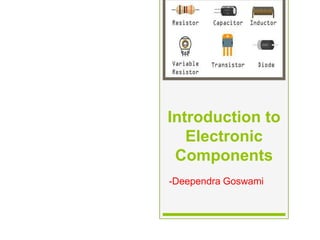
  • 2. Electronic Component : Electronic component is basic fundamental building block of any electronic system precisely used to affect electrons and their associated fields. Each component may have one or more basic properties and it behaves accordingly.
  • 4. Active Components  Active components are those which conduct upon providing some external energy i.e. require electrical power to operate.  Usually they inject power into the circuit.  Examples – Diodes, Transister, ICs, Transformer etc.
  • 5. DIODES  Diode is a one way valve for electricity.  It is a two terminal semiconductor device, these two terminals are called the anode and cathode.  It lets the electricity to flow only in one direction.
  • 6.  Most diodes have painted line on one end showing the direction or flow. The negative side is normally white  Current flow through diode only when positive voltage is applied to anode and negative voltage is connected to cathode  If these voltages are reversed, then the current will not flow.
  • 9. LIGHT EMITTING DIODE (LED)  This is one of the most popular diodes used in our daily life.  This is also a normal PN junction diode except instead of silicone and germanium, the materials like gallium arsenide, gallium arsenide phosphide used in construction.
  • 11. WORKING PRINCIPLE OF LED  Like a normal PN junction diode, this is connected in forward bias condition so that the diode conducts.  The conduction takes place in a LED when the free electrons in the conduction band combine with the holes in the valence band. This process of recombination emits light. This process is called as Electroluminescence.
  • 12.  The color of the light emitted depends upon the gap between the energy bands.  The materials used also effect the colors like, gallium arsenide phosphide emits either red or yellow, gallium phosphide emits either red or green and gallium nitrate emits blue light. Whereas gallium arsenide emits infrared light.  The LEDs for non-visible Infrared light are used mostly in remote controls.
  • 13. TRANSISTOR  A transistor is a 3 three terminal semiconductor device in which a voltage is applied to one of the terminal (called base) can control current that flows across the other two terminals (called collector and base).  These 3 terminals are called Emitter, Base and Collector
  • 14.  It is a fundamental building block of circuitory in mobile phones, computers, and several other electronic devices.  Transistor has very fast response and is used in number of functions including voltage regulations, amplification, switching, oscillators etc.  Transistors may be packed individually or they can be a part of an IC (integrated circuit).  Some of the ICs have billions of transistors ia very small area.
  • 15. TYPES OF TRANSISTORS  NPN : When a P-type semiconductor is sandwitched between two N-type semiconductor then it is called NPN. Majority charge carriers are electrons.  PNP : When a N-type semiconductor is sandwitched between two P-type semiconductor then it is called NPN. Majority charge carriers are holes.
  • 16. FIELD EFFECT TRANSISTORS (FET)  The FET is a transistor that uses a electric field to control the electrical behaviour of device.  FET s are also known as unipolar transistors since they involve single carrier type operation.  The device consist of an active channel through which charge carriers, electrons or holes flow from source to drain.  The conductivity of channel is function of potential applied across the gate and source terminals.
  • 17.  FET’s 3 terminals are : 1. Source(S), through which the carriers enter the channel. Conventionally, the current entering the channel is designated by Is. 2. Drain(D), through which the carriers leave the channel. Conventionally, the current entering the drain is designated by ID. Drain to source voltage is VDS. 3. Gate(G), the terminal that modulates the channel conductivity. By applying voltage to G one can control ID.
  • 18. TYPES OF FET s  The JFET : Junction field effect transistor  The MOSFET : Metal oxide semiconductor field effect transistor  The MNOS: Metal nitride oxide semiconductor transistor  The DGMOSFET : Dual gate MOSFET  The MODFET : Modulation doped FET  The TFET : Tunnel field effect Transistor etc.
  • 19. MOSFET  MOSFET stands for Metal Oxide Silicon Field Effect Transistor or Metal Oxide Semiconductor Field Effect Transistor.  This is also called as IGFET meaning Insulated Gate Field Effect Transistor.  The FET is operated in both depletion and enhancement modes of operation.
  • 20.  The following figure shows how a practical MOSFET looks like.
  • 21. CONSTRUCTION OF MOSFET  The construction of a MOSFET is a bit similar to the JFET .  An oxide layer is deposited on the substrate to which the gate terminal is connected. This oxide layer acts as an insulator (sio2 insulates from the substrate), and hence the MOSFET has another name as IGFET (Insulated gate FET).  With negative gate bias voltage, it acts as depletion MOSFET while with positive gate bias voltage it acts as an Enhancement MOSFET.
  • 22.  The following figure shows the construction of a MOSFET .
  • 23.  The voltage at gate controls the operation of the MOSFET . In this case, both positive and negative voltages can be applied on the gate as it is insulated from the channel.  In the construction of MOSFET , a lightly doped substrate, is diffused with a heavily doped region. Depending upon the substrate used, they are called as P-type and N-type MOSFET s.
  • 24. CLASSIFICATION OF MOSFET  Depending upon the type of materials used in the construction, and the type of operation, the MOSFET s are classified as in the following figure.
  • 25. N-MOSFET  Let us consider an N-channel MOSFET to understand its working. A lightly doped P-type substrate is taken into which two heavily doped N-type regions are diffused, which act as source and drain.  Between these two N+ regions, there occurs diffusion to form an N-channel, connecting drain and source.  A thin layer of Silicon dioxide (SiO2) is grown over the entire surface and holes are made to draw ohmic contacts for drain and source terminals.
  • 27.  A conducting layer of aluminum is laid over the entire channel, upon this SiO2layer from source to drain which constitutes the gate. The SiO2 substrate is connected to the common or ground terminals.  Because of its construction, the MOSFET has a very less chip area than BJT , which is 5% of the occupancy when compared to bipolar junction transistor. This device can be operated in modes. They are depletion and enhancement modes.
  • 28. Working of N - Channel (depletion mode) MOSFET  For now, we have an idea that there is no PN junction present between gate and channel in this, unlike a FET .
  • 29. together form a parallel plate capacitor. get attracted and settle near SiO2 layer. But the  We can also observe that, the diffused channel N (between two N+ regions), the insulating dielectric SiO2 and the aluminum metal layer of the gate  If the NMOS has to be worked in depletion mode, the gate terminal should be at negative potential while drain is at positive potential.  When no voltage is applied between gate and source, some current flows due to the voltage between drain and source. Let some negative voltage is applied at VGG. Then the minority carriers i.e. holes, majority carriers, i.e., electrons get repelled.
  • 30.  With some amount of negative potential at VGG a certain amount of drain current ID flows through source to drain.  When this negative potential is further increased, the electrons get depleted and the current ID decreases. Hence the more negative the applied VGG, the lesser the value of drain current ID will be.  The channel nearer to drain gets more depleted than at source (like in FET) and the current flow decreases due to this effect. Hence it is called as depletion mode MOSFET .
  • 31. Working of N - Channel (Enhancement mode) MOSFET  The same MOSFET can be worked in enhancement mode, if we can change the polarities of the voltage VGG. So, let us consider the MOSFET with gate source voltage VGG being positive as shown in the following figure.
  • 32. carriers i.e. holes, get repelled and the majority carriers i.e. of drain current ID flows through source to drain. these are pushed further due to the voltage applied at VGG. drain current ID will be.  When no voltage is applied between gate and source, some current flows due to the voltage between drain and source.  Let some positive voltage is applied at VGG. Then the minority electrons gets attracted towards the SiO2 layer.  With some amount of positive potential at VGG a certain amount  When this positive potential is further increased, the current ID increases due to the flow of electrons from source and  Hence the more positive the applied VGG, the more the value of  The current flow gets enhanced due to the increase in electron flow better than in depletion mode. Hence this mode is termed as Enhanced Mode MOSFET.
  • 33.  Hence the more positive the applied VGG, the more the value of drain current ID will be.  The current flow gets enhanced due to the increase in electron flow better than in depletion mode. Hence this mode is termed as Enhanced Mode MOSFET.
  • 34. P-MOSFET  The construction and working of a PMOS is same as NMOS. A lightly doped n-substrate is taken into which two heavily doped P+ regions are diffused.  These two P+ regions act as source and drain. A thin layer of SiO2 is grown over the surface.  Holes are cut through this layer to make contacts with P+ regions, as shown in the following figure.
  • 36. DRAIN CHARACTERSTICS  The drain characteristics of a MOSFET are drawn between the drain current ID and the drain source voltage VDS. The characteristic curve is as shown below for different values of inputs.
  • 37. TRANSFER CHARACTERSTICS  Transfer characteristics define the change in the value of VDS with the change in ID and VGS in both depletion and enhancement modes. The below transfer characteristic curve is drawn for drain current versus gate to source voltage.
  • 38. - Noninverting OP-AMP (IC-741)  An operational amplifier is a direct-coupled high-gain amplifier.  It offers the gain of the order of 106. +VCC Inverting input Op-Amp output IC-741 + input -VEE
  • 39. circuit package. excitation/input, 1 pin is not used hence named IC-741. and followed by a level translator and an output stage.  An operational amplifier is available as a single integrated  There are 8 pins in it, 7 pins are active, 4 pins are for  It usually consisting of one or more differential amplifiers  It is a versatile device that an amplify DC as well as AC. PIN DIAGRAM
  • 40. IDEAL OP-AMP CHARACTERSTICS  Infinite voltage gain.  Infinite input resistance so that almost any signal source can drive it and there is no loading on the preceding stage.  Zero output resistance so that output can drive an infinite number of other devices.  Infinite bandwidth so that any frequency signal from 0 to ∞ Hz can be amplified without attenuation.  Infinite CMRR so that the output common-mode noise voltage is zero.  Infinite slew rate so that output voltage changes occur simultaneously with input voltage changes.
  • 41. Equivalent Circuit of Op-Amp Vo =Ad (V1-V2) = AdVd The op-amp amplifies the difference between the two input voltages. It does not amplify the input voltages themselves. The polarity of the output voltage depends on the polarity of the difference voltage Vd.
  • 42. Ideal Voltage Transfer Characteristics
  • 43. O/P LEVEL Internal Circuit Of Op-Amp NON INVERTING I/P INPUT INTERMEDIAT SHIFTING OUTPUT STAGE E STAGE STAGE INVERTING I/P STAGE DUAL I/P DUAL I/P EMITTER DUAL I/P BALANCED O/P UNBALANCED FOLLOWER CIRCUIT BALANCED O/P DIFFERENTIAL O/P USING CONSTANT DIFFERENTIAL AMPLIFIER DIFFERENTIAL CURRENT SOURCE AMPLIFIER AMPLIFIER
  • 44. amplifier. This stage generally provides most of resistance of the op-amp. the voltage amplifier, which is driven by the output of the first stage. On unbalanced output. the intermediate stage is well above ground potential. the intermediate stage downwards to zero volts with respect symmetry amplifier output stage. The output stage increases capabilities of the op-amp. resistance. Continued....  The input stage is the dual input balanced output differential gain of the amplifier and also establishes the input  The intermediate stage is usually another differential most amplifiers, the intermediate stage is dual input,  Because of direct coupling, the dc voltage at the output of Therefore, the level translator (shifting) circuit is used after to ground.  The final stage is usually a push pull complementary the Voltage swing and raises the ground supplying  A well designed Output stage also provides low output
  • 45. APPLICATIONS  It was originally designed for computing such mathematical functions as addition, subtraction, multiplication, and integration.  Thus the name operational amplifier stems from its original use for these mathematical operations and is abbreviated to op-amp.  With the addition of suitable external feedback components, the modern day op-amp can be used for a variety of applications, such as ac and dc signal amplification, active filters, oscillators, comparators, regulators, and others.
  • 46.  For e.g. measurements of temperature and humidity inside  Its one of the important application is in construction of instrumentation amplifier. INSTRUMENTATION AMPLIFIER  In many industrial and consumer applications the measurement and control of physical conditions are very important.  For e.g. measurements of temperature and humidity insi a dairy or meat plant permit the operator to make necessary adjustments to maintain product quality.  Similarly, precise temperature control of plastic furnace is needed to produce a particular type of plastic.
  • 47. CIRCUIT DIAGRAM OF INSTRUMENTATION APMLIFIER
  • 48. OUTPUT INTERMEDIA T INPUT APPLICATION Quantity to be measured O/P STAGE E STAGE STAGE Transducer + Instrumentation Indicator and Preamplifier Amplifier automatic process controller Transmssion line
  • 49. Continued…  Some transducers produce outputs with sufficient strength to perform their use directly, many do not.  T o amplify the low-level output signal of the transducer so that it can drive the indicator or display is the major function of the instrumentation amplifier.  The instrumentation amplifier is intended for precise, low-level signal amplification where low noise, low thermal and time drifts, high input resistance, and accurate closed-loop gain are required. Besides, low power consumption, high common-mode rejection ratio, and high slew rate are desirable for superior performance.
  • 50. TIMER (IC-555)  IC 555 was Introduced in 1970 by SIGNATICS corporation.  It is used for generation of square wave (asymmetric and symmetric), saw tooth, and various other applications such as Astable, Monostable, and Bistable multivibrator.  The most versatile linear integrated circuits is the 555 timer.
  • 51. accurate and highly stable time delays or oscillation. DIP . as monostable (one-shot) multivibrator or as an astable (free on +5 to + 18 V supply voltage in both free-running (astable) cycle; timing is from microseconds through hours; it has a astable multivibrators, dc-dc converters, digital logic probes, tachometers, temperature measurement and control, infrared electric eyes, and many others.  The 555 is a monolithic timing circuit that can produce  The device is available as an 8-pin metal can, an 8-pin mini  The timer basically operates in one of the two modes: either running) multivibrator.  The important features of the 555 timer are these: it operates and one- shot (monostable) modes; it has an adjustable duty high current output; it can source or sink 200 mA.  A sample of these applications includes mono-stable and waveform generators, analog frequency meters and transmitters, burglar and toxic gas alarms, voltage regulators,
  • 53. FUNCTIONAL BLOCK DIAGRAM OF 555 TIMER 2/3 Vcc 1/3 Vcc
  • 54. PIN DESCRIPTION AND WORKING  Pin 1: Ground All voltages are measured with respect to this terminal.  Pin 2: Trigger The output of the timer depends on the amplitude of the external trigger pulse applied to this pin. The output is low if the voltage at this pin is greater than 2/3 VCC. However, when a negative-going pulse of amplitude larger than 1/3 VCC is applied to this pin, the comparator 2 output goes low, which in turn switches the output of the timer high. The output remains high as long as the trigger terminal is held at a low voltage.
  • 55.  Pin 3: Output There are two ways a load can be connected to the output terminal: either between pin 3 and ground (pin 1) or between pin 3 and supply voltage +VCC (pin 8). When the output is low, the load current flows through the load connected between pin 3 and +VCC into the terminal and is called the sink current. However, the current through the grounded load is zero when the output is low. For this reason, the load connected between pin 3 and +VCC is called the normally on load and that connected between pin 3 and ground is called the normally off load. On the other hand, when the output is high, the current through the load connected between pin 3and + VCC (normally on load) is zero. However, the output terminal supplies current to the normally off load. This current is called the source current. The maximum value of sink or source current is 200 mA.
  • 56.  Pin 4: Reset. The 555 timer can be reset (disabled) by applying a negative pulse to this pin. When the reset function is not in use, the reset terminal should be connected to + VCC to avoid any possibility of false triggering.  Pin 5: Control voltage An external voltage applied to this terminal changes the threshold as well as the trigger voltage . In other words, by imposing a voltage on this pin or by connecting a pot between this pin and ground, the pulse width of the output waveform can be varied. When not used, the control pin should be bypassed to ground with a 0.01-μF capacitor to prevent any noise problems.
  • 57.  Pin 6: Threshold This is the non-inverting input terminal of comparator 1, which monitors the voltage across the external capacitor. When the voltage at this pin is threshold voltage 2/3 V, the output of comparator 1 goes high, which in turn switches the output of the timer low.  Pin 7: Discharge This pin is connected internally to the collector of transistor, When the output is high, Transistor is off and acts as an open circuit to the external capacitor C connected across it. On the other hand, when the output is low, Q1 is saturated and acts as a short circuit, shorting out the external capacitor C to ground.  Pin 8: + VCC The supply voltage of +5 V to +18 is applied to this pin with respect to ground (pin 1).
  • 59. Passive Components  Passive electronic components are those that don’t have the ability to control current by means of another signal.  They start their operation once they are connected.  No external energy is needed for their operation.  E.g. Resistors, capacitors, inductors, LDR etc.
  • 60. RESISTOR  It is device that resists the flow of current.  Resistors comes in variety of resistance values(how much they resist current, measured in unit called ohm) and power rating (how much power they can handle without burning up, measured in watts).
  • 62. POTENTIOMETER  A potentiometer is a 3 terminal resistor with a sliding or rotating contact that forms an adjustable voltage divider.  If only two terminals are used, one end and the wiper, it act as a variable resistor
  • 63. LIGHT DEPENDENT RESISTOR (LDR)  An LDR is a component that has a (variable) resistance that change with the light intensity that falls upon it.  This allows them to be used in light sensing circuits.
  • 64. CAPACITOR  It is a device that can temporarily store an electric charge.  Capacitors come in several varieties, the two most common being ceramic disk and electrolyte.  The amount of capacitance of a given capacitor is usually measured in micro farads, uf.
  • 65. INDUCTOR  An inductor is also called a coil, choke, or reactor, is a passive two terminal electrical component that stores energy in form of magnetic field when electric current flows through it.  An inductor typically consists of an insulated wire wound into a coil around a core.
  • 67. LOGIC GATES  Logic gates are the basic building blocks of any digital system.  It is an electronic circuit having one or more than one input and only one output.  At any given moment, every terminal is in one of the two binary conditions low (0) or high (1), represented by different voltage levels.  The relationship between the input and the output is based on a certain logic.  Based on this, There are 7 different logic gates : AND, OR, NOT , NAND, NOR, XOR, XNOR etc.
  • 68.
  • 69. uth table: AND GATE  A circuit which performs an AND operation is shown in figure. It has n input (n >= 2) and one output.  Logic diagram:  Tr
  • 70. OR GATE  A circuit which performs an OR operation is shown in figure. It has n input (n >= 2) and one output.  Logic diagram:  Truth table:
  • 71. NOT GATE  NOT gate is also known as Inverter. It has one input A and one output Y .  Logic diagram:  Truth table:
  • 72. NAND GATE  A NOT-AND operation is known as NAND operation. It has n input (n >= 2) and one output.  Logic diagram:  Truth table:
  • 73. NOR GATE  A NOT-OR operation is known as NOR operation. It has n input (n >= 2) and one output.  Logic diagram:  Truth table:
  • 74. Truth table: XOR GATE  XOR or Ex-OR or exclusive-OR gate is a special type of gate. It can be used in the half adder, full adder and subtractor. It has n input (n >= 2) and one output.  Logic diagram: 
  • 75. XNOR GATE  XNOR or EX- NOR or exclusive-NOR gate is a special type of gate. It can be used in the half adder, full adder and subtractor. It has n input (n >= 2) and one output.  Logic diagram:  Truth table:
  • 76. DC TO DC BOOSTER CIRCUIT OR BOOST CONVERTER  A process that changes one DC voltage to a different DC voltage is called DC to DC conversion.  A boost converter is a DC to DC converter with output voltage greater than the source voltage.  A boost converter is sometimes called step-up converter since it “steps-up” the source voltage.  DC to DC boosters are available as ICs requiring few more components and are also available as complete hybrid circuit modules, ready for use with in a electronic assembly.
  • 77. THE BASIC SCHEMATIC OF DC TO DC BOOST CONVERTER