SlideShare a Scribd company logo
1 of 24
11/22/2023 ASIC Design Flow 1
ASIC Design Flow
Prof Usha Mehta
Professor and PG Coordinator (VLSI Design)
Institute of Technology, Nirma University, Ahmedabad
usha.mehta@nirmauni.ac.in
11/22/2023 ASIC Design Flow 2
Acknowledgement….
• This presentation has been summarized from various
books, papers, websites and presentations related to
the topic all over the world. I couldn’t remember where
these large pull of hints and work come from. However,
I’d like to thank all professors and scientists who
created such a good work on this emerging field.
Without those efforts in this very emerging technology,
these notes and slides can’t be finished.
11/22/2023 ASIC Design Flow 3
Basic
ASIC Design Flow
11/22/2023 ASIC Design Flow 4
11/22/2023 ASIC Design Flow 5
• The above basic design flow is somehow over simplified
in the sense that it only connects the design tasks in one
direction.
• Interactions between different stages, especially the
influences of later stages on earlier ones, are not shown.
• In reality, a design cannot be done in such a singular
path.
– If the timing analysis finds that the delay of the critical
path is longer than that required by a clock period, we
have to go back to the physical design to modify the
layout.
– If the problem cannot be resolved inside the physical
design stage we then have to go back further to the
circuit design to add buffers.
– If we cannot resolve the problem through the
modification of physical or circuit design, we would have
to go back another stage to change the architecture
design.
11/22/2023 ASIC Design Flow 6
• Most interference between different design stages is
actually due to system performance requirements and
variable remitting solutions at different stages.
– As a consequence, we need to have loops in the
design flow.
• In general we want to go backward as little as
possible.
– A subsequent problem is that we might be end up
cycling through these stages endlessly.
– This issue is called timing closure
11/22/2023 ASIC Design Flow 7
Timing Closure
11/22/2023 ASIC Design Flow 8
Verification
and Testing
11/22/2023 ASIC Design Flow 9
System Specification
• A real ASIC design practice starts from understanding
the application and writing a clear and complete
specification in terms of VLSI terminology, such as
input/output signals, clock rate, protocol definition,
operation mode and etc.
• Writing a specification for an ASIC project includes
– Understanding the application
– Communicating with customer for whom ASIC chip
is designed
– Converting application terminology into circuit
design terminology
– Defining system settings
– Listing the performance criteria, and
– Selecting the process
11/22/2023 ASIC Design Flow 10
Architectural Design
• Architecture design
• Architecture probably plays the most important role in
determining the quality of a designed chip.
• Experience in IC design and insight into the
application contribute to the architecture choice.
• Currently, architecture design still depends on the wisdom
of the designer instead of on CAD tools, since there are too
many factors involved.
• Unfortunately the influence of different factors usually
conflicts with each other.
• Decisions on the architecture, e.g., RISC/CISC, # of
ALU’s, pipeline structure, cache size, etc. Such
decisions can provide an accurate estimation of the
system performance, die size, power consumption, etc.
11/22/2023 ASIC Design Flow 11
Functional/Behavioural Design
• Identify main functional units and their
interconnections. No details of implementation.
• Functional design is generally done with HDL
11/22/2023 ASIC Design Flow 12
Register Transfer Level
+
+
0010
0001
0100
0011
• Components, data types
• Design the logic, e.g., Boolean expressions,
control flow, word width, register
allocation, etc.
• RTL is expressed in a HDL mostly
synthesized from behavioral description
11/22/2023 ASIC Design Flow 13
Logic Level
• Discrete Level, Discrete Time
• Design the circuit including gates, transistors,
interconnections, etc. The outcome is called a netlist.
• Homework
ISCAS Gate level
Netlist
11/22/2023 ASIC Design Flow 14
Circuit level
• Continuous Voltage, Continuous time
11/22/2023 ASIC Design Flow 15
Layout
• Convert the netlist into a geometric representation. The
outcome is called a layout.
11/22/2023 ASIC Design Flow 16
Few more words…
• Circuit Partitioning – Partition a large circuit into sub-
circuits (called blocks). Factors like #blocks, block
sizes, interconnection between blocks, etc., are
considered.
• Floorplanning – Set up a plan for a good layout. Place
the modules (modules can be blocks, functional units,
etc.) at an early stage when details like shape, area,
I/O pin positions of the modules, …, are not yet fixed.
• Placement – Exact placement of the modules (modules
can be gates, standard cells, etc.) when details of the
module design are known. The goal is to minimize the
delay, total area and interconnect cost.
11/22/2023 ASIC Design Flow 17
• Routing – Complete the interconnections between
modules. Factors like critical path, clock skew, wire
spacing, etc., are considered. Include global routing
and detailed routing.
• Compaction – Compress the layout from all directions
to minimize the total chip area.
• Verification – Check the correctness of the layout.
Include DRC (Design Rule Checking), circuit extraction
(generate a circuit from the layout to compare with the
original netlist), performance verification (extract
geometric information to compute resistance,
capacitance, delay, etc.)
11/22/2023 ASIC Design Flow 18
Cont….
• Logic Synthesizer
• Translation from RTL specification to netlist
• Adequate for the design that do not have critical
performance parameter
• Provides room to make design improvement
• Understanding of device architecture is necessary
• Gate Level Simulation
• To ensure correctness of synthesis translation
• Vendor supplied parameters are used to simulate the
actual target device parameters
11/22/2023 ASIC Design Flow 19
Cont…
• Extraction
• Actual resistance and capacitance figures modelled for
interconnections are extracted to simulate timing
performance
• Post Layout Simulation
• Functionality taking care of timings
• Time extraction imported
• Both gate and interconnection delays are considered
• Back Annotation
• To update the initial circuit data with information that
was obtained later in the design cycle
• Passing the information related to the extra load that
may occur in practice
11/22/2023 ASIC Design Flow 20
Cont…
• Extended Testing
• For ASIC, GA, SoG.
• Not for FPGA
• Device Programming
• Via JTAG port
• For FPGA
11/22/2023 ASIC Design Flow 21
VLSI Design Tools
• By Chip vendor
• By third party
• Cadence
• Mentor Graphics
• Synopsis
• Microwind
11/22/2023 ASIC Design Flow 22
11/22/2023 ASIC Design Flow 23
Coverage of my area….
• ASIC
• Full Custom
• CMOS Design
• Simulation
• Layout
• SemiCustom
• Verification
• Gate Array
• Std. Cell
• DFT
• STA
• FP-Floor Plan
• CTC – Clock Tree
Synthesis
• FPGA
• HDL Entry
• Place and Route
11/22/2023 ASIC Design Flow 24
Thank you!

More Related Content

What's hot

Placement in VLSI Design
Placement in VLSI DesignPlacement in VLSI Design
Placement in VLSI DesignTeam-VLSI-ITMU
 
2 when to_test_role_of_testing
2 when to_test_role_of_testing2 when to_test_role_of_testing
2 when to_test_role_of_testingUsha Mehta
 
Digital VLSI Design : Introduction
Digital VLSI Design : IntroductionDigital VLSI Design : Introduction
Digital VLSI Design : IntroductionUsha Mehta
 
Static_Timing_Analysis_in_detail.pdf
Static_Timing_Analysis_in_detail.pdfStatic_Timing_Analysis_in_detail.pdf
Static_Timing_Analysis_in_detail.pdfUsha Mehta
 
1 introduction to vlsi physical design
1 introduction to vlsi physical design1 introduction to vlsi physical design
1 introduction to vlsi physical designsasikun
 
2019 3 testing and verification of vlsi design_sta
2019 3 testing and verification of vlsi design_sta2019 3 testing and verification of vlsi design_sta
2019 3 testing and verification of vlsi design_staUsha Mehta
 
Sta by usha_mehta
Sta by usha_mehtaSta by usha_mehta
Sta by usha_mehtaUsha Mehta
 
Testing and Verification of Electronics Circuits : Introduction
Testing and Verification of Electronics Circuits : IntroductionTesting and Verification of Electronics Circuits : Introduction
Testing and Verification of Electronics Circuits : IntroductionUsha Mehta
 
Multi mode multi corner (mmmc)
Multi mode multi corner (mmmc)Multi mode multi corner (mmmc)
Multi mode multi corner (mmmc)shaik sharief
 
Introduction of testing and verification of vlsi design
Introduction of testing and verification of vlsi designIntroduction of testing and verification of vlsi design
Introduction of testing and verification of vlsi designUsha Mehta
 
Flip Chip technology
Flip Chip technologyFlip Chip technology
Flip Chip technologyMantra VLSI
 
Vlsi interview questions compilation
Vlsi interview questions compilationVlsi interview questions compilation
Vlsi interview questions compilationRajesh M
 
Implementing Useful Clock Skew Using Skew Groups
Implementing Useful Clock Skew Using Skew GroupsImplementing Useful Clock Skew Using Skew Groups
Implementing Useful Clock Skew Using Skew GroupsM Mei
 
Physical Verification Design.pdf
Physical Verification Design.pdfPhysical Verification Design.pdf
Physical Verification Design.pdfAhmed Abdelazeem
 
VLSI-Physical Design- Tool Terminalogy
VLSI-Physical Design- Tool TerminalogyVLSI-Physical Design- Tool Terminalogy
VLSI-Physical Design- Tool TerminalogyMurali Rai
 

What's hot (20)

Placement in VLSI Design
Placement in VLSI DesignPlacement in VLSI Design
Placement in VLSI Design
 
2 when to_test_role_of_testing
2 when to_test_role_of_testing2 when to_test_role_of_testing
2 when to_test_role_of_testing
 
Digital VLSI Design : Introduction
Digital VLSI Design : IntroductionDigital VLSI Design : Introduction
Digital VLSI Design : Introduction
 
Static_Timing_Analysis_in_detail.pdf
Static_Timing_Analysis_in_detail.pdfStatic_Timing_Analysis_in_detail.pdf
Static_Timing_Analysis_in_detail.pdf
 
1 introduction to vlsi physical design
1 introduction to vlsi physical design1 introduction to vlsi physical design
1 introduction to vlsi physical design
 
2019 3 testing and verification of vlsi design_sta
2019 3 testing and verification of vlsi design_sta2019 3 testing and verification of vlsi design_sta
2019 3 testing and verification of vlsi design_sta
 
Sta by usha_mehta
Sta by usha_mehtaSta by usha_mehta
Sta by usha_mehta
 
Testing and Verification of Electronics Circuits : Introduction
Testing and Verification of Electronics Circuits : IntroductionTesting and Verification of Electronics Circuits : Introduction
Testing and Verification of Electronics Circuits : Introduction
 
Multi mode multi corner (mmmc)
Multi mode multi corner (mmmc)Multi mode multi corner (mmmc)
Multi mode multi corner (mmmc)
 
Introduction of testing and verification of vlsi design
Introduction of testing and verification of vlsi designIntroduction of testing and verification of vlsi design
Introduction of testing and verification of vlsi design
 
Powerplanning
PowerplanningPowerplanning
Powerplanning
 
Flip Chip technology
Flip Chip technologyFlip Chip technology
Flip Chip technology
 
Inputs of physical design
Inputs of physical designInputs of physical design
Inputs of physical design
 
STA.pdf
STA.pdfSTA.pdf
STA.pdf
 
Vlsi interview questions compilation
Vlsi interview questions compilationVlsi interview questions compilation
Vlsi interview questions compilation
 
Implementing Useful Clock Skew Using Skew Groups
Implementing Useful Clock Skew Using Skew GroupsImplementing Useful Clock Skew Using Skew Groups
Implementing Useful Clock Skew Using Skew Groups
 
Clock Tree Synthesis.pdf
Clock Tree Synthesis.pdfClock Tree Synthesis.pdf
Clock Tree Synthesis.pdf
 
Physical Verification Design.pdf
Physical Verification Design.pdfPhysical Verification Design.pdf
Physical Verification Design.pdf
 
VLSI-Physical Design- Tool Terminalogy
VLSI-Physical Design- Tool TerminalogyVLSI-Physical Design- Tool Terminalogy
VLSI-Physical Design- Tool Terminalogy
 
Pd flow i
Pd flow iPd flow i
Pd flow i
 

Similar to 2_DVD_ASIC_Design_FLow.pdf

Fpga asic technologies_flow
Fpga asic technologies_flowFpga asic technologies_flow
Fpga asic technologies_flowravi4all
 
VLSI Physical Design Automation.ppt
VLSI Physical Design Automation.pptVLSI Physical Design Automation.ppt
VLSI Physical Design Automation.pptRichikDey5
 
Making of an Application Specific Integrated Circuit
Making of an Application Specific Integrated CircuitMaking of an Application Specific Integrated Circuit
Making of an Application Specific Integrated CircuitSWINDONSilicon
 
SISTec Microelectronics VLSI design
SISTec Microelectronics VLSI designSISTec Microelectronics VLSI design
SISTec Microelectronics VLSI designDr. Ravi Mishra
 
13257474.ppt-it-networking-gdfgdfgdfgdbd
13257474.ppt-it-networking-gdfgdfgdfgdbd13257474.ppt-it-networking-gdfgdfgdfgdbd
13257474.ppt-it-networking-gdfgdfgdfgdbdssuser38ba4b
 
VLSI unit 1 Technology - S.ppt
VLSI unit 1 Technology - S.pptVLSI unit 1 Technology - S.ppt
VLSI unit 1 Technology - S.pptindrajeetPatel22
 
Krishnakumar signalling
Krishnakumar signallingKrishnakumar signalling
Krishnakumar signallingKrishna Kumar
 
ASIC design Flow (Digital Design)
ASIC design Flow (Digital Design)ASIC design Flow (Digital Design)
ASIC design Flow (Digital Design)Sudhanshu Janwadkar
 
Vlsi physical design-notes
Vlsi physical design-notesVlsi physical design-notes
Vlsi physical design-notesDr.YNM
 
VLSI UNIT-1.1.pdf.ppt
VLSI UNIT-1.1.pdf.pptVLSI UNIT-1.1.pdf.ppt
VLSI UNIT-1.1.pdf.pptrajukolluri
 
unit 1vlsi notes.pdf
unit 1vlsi notes.pdfunit 1vlsi notes.pdf
unit 1vlsi notes.pdfAcademicICECE
 
Lecture20 asic back_end_design
Lecture20 asic back_end_designLecture20 asic back_end_design
Lecture20 asic back_end_designHung Nguyen
 
High speed-pcb-board-design-and-analysiscadence-130218085524-phpapp01
High speed-pcb-board-design-and-analysiscadence-130218085524-phpapp01High speed-pcb-board-design-and-analysiscadence-130218085524-phpapp01
High speed-pcb-board-design-and-analysiscadence-130218085524-phpapp01khalid noman husainy
 
10 static timing_analysis_1_concept_of_timing_analysis
10 static timing_analysis_1_concept_of_timing_analysis10 static timing_analysis_1_concept_of_timing_analysis
10 static timing_analysis_1_concept_of_timing_analysisUsha Mehta
 

Similar to 2_DVD_ASIC_Design_FLow.pdf (20)

Chapter1.slides
Chapter1.slidesChapter1.slides
Chapter1.slides
 
Fpga asic technologies_flow
Fpga asic technologies_flowFpga asic technologies_flow
Fpga asic technologies_flow
 
VLSI Physical Design Automation.ppt
VLSI Physical Design Automation.pptVLSI Physical Design Automation.ppt
VLSI Physical Design Automation.ppt
 
Making of an Application Specific Integrated Circuit
Making of an Application Specific Integrated CircuitMaking of an Application Specific Integrated Circuit
Making of an Application Specific Integrated Circuit
 
Hierarchical design and design abstraction
Hierarchical design and design abstractionHierarchical design and design abstraction
Hierarchical design and design abstraction
 
SISTec Microelectronics VLSI design
SISTec Microelectronics VLSI designSISTec Microelectronics VLSI design
SISTec Microelectronics VLSI design
 
13257474.ppt-it-networking-gdfgdfgdfgdbd
13257474.ppt-it-networking-gdfgdfgdfgdbd13257474.ppt-it-networking-gdfgdfgdfgdbd
13257474.ppt-it-networking-gdfgdfgdfgdbd
 
VLSI unit 1 Technology - S.ppt
VLSI unit 1 Technology - S.pptVLSI unit 1 Technology - S.ppt
VLSI unit 1 Technology - S.ppt
 
VLSI design flow.pptx
VLSI design flow.pptxVLSI design flow.pptx
VLSI design flow.pptx
 
Krishnakumar signalling
Krishnakumar signallingKrishnakumar signalling
Krishnakumar signalling
 
ASIC design Flow (Digital Design)
ASIC design Flow (Digital Design)ASIC design Flow (Digital Design)
ASIC design Flow (Digital Design)
 
Vlsi physical design-notes
Vlsi physical design-notesVlsi physical design-notes
Vlsi physical design-notes
 
VLSI UNIT-1.1.pdf.ppt
VLSI UNIT-1.1.pdf.pptVLSI UNIT-1.1.pdf.ppt
VLSI UNIT-1.1.pdf.ppt
 
unit 1vlsi notes.pdf
unit 1vlsi notes.pdfunit 1vlsi notes.pdf
unit 1vlsi notes.pdf
 
VLSI Design- Guru.ppt
VLSI Design- Guru.pptVLSI Design- Guru.ppt
VLSI Design- Guru.ppt
 
Lecture20 asic back_end_design
Lecture20 asic back_end_designLecture20 asic back_end_design
Lecture20 asic back_end_design
 
High speed-pcb-board-design-and-analysiscadence-130218085524-phpapp01
High speed-pcb-board-design-and-analysiscadence-130218085524-phpapp01High speed-pcb-board-design-and-analysiscadence-130218085524-phpapp01
High speed-pcb-board-design-and-analysiscadence-130218085524-phpapp01
 
VLSI GDI Technology
VLSI GDI TechnologyVLSI GDI Technology
VLSI GDI Technology
 
System on Chip (SoC)
System on Chip (SoC)System on Chip (SoC)
System on Chip (SoC)
 
10 static timing_analysis_1_concept_of_timing_analysis
10 static timing_analysis_1_concept_of_timing_analysis10 static timing_analysis_1_concept_of_timing_analysis
10 static timing_analysis_1_concept_of_timing_analysis
 

More from Usha Mehta

Basic Design Flow for Field Programmable Gate Arrays
Basic Design Flow for Field Programmable Gate ArraysBasic Design Flow for Field Programmable Gate Arrays
Basic Design Flow for Field Programmable Gate ArraysUsha Mehta
 
5_DVD_VLSI Technology Trends.pdf
5_DVD_VLSI Technology Trends.pdf5_DVD_VLSI Technology Trends.pdf
5_DVD_VLSI Technology Trends.pdfUsha Mehta
 
13_DVD_Latch-up_prevention.pdf
13_DVD_Latch-up_prevention.pdf13_DVD_Latch-up_prevention.pdf
13_DVD_Latch-up_prevention.pdfUsha Mehta
 
14 static timing_analysis_5_clock_domain_crossing
14 static timing_analysis_5_clock_domain_crossing14 static timing_analysis_5_clock_domain_crossing
14 static timing_analysis_5_clock_domain_crossingUsha Mehta
 
9 semiconductor memory
9 semiconductor memory9 semiconductor memory
9 semiconductor memoryUsha Mehta
 
13 static timing_analysis_4_set_up_and_hold_time_violation_remedy
13 static timing_analysis_4_set_up_and_hold_time_violation_remedy13 static timing_analysis_4_set_up_and_hold_time_violation_remedy
13 static timing_analysis_4_set_up_and_hold_time_violation_remedyUsha Mehta
 
12 static timing_analysis_3_clocked_design
12 static timing_analysis_3_clocked_design12 static timing_analysis_3_clocked_design
12 static timing_analysis_3_clocked_designUsha Mehta
 
11 static timing_analysis_2_combinational_design
11 static timing_analysis_2_combinational_design11 static timing_analysis_2_combinational_design
11 static timing_analysis_2_combinational_designUsha Mehta
 
6 verification tools
6 verification tools6 verification tools
6 verification toolsUsha Mehta
 
5 verification methods
5 verification methods5 verification methods
5 verification methodsUsha Mehta
 
4 verification flow_planning
4 verification flow_planning4 verification flow_planning
4 verification flow_planningUsha Mehta
 
3 test economic_test_equipments_yield
3 test economic_test_equipments_yield3 test economic_test_equipments_yield
3 test economic_test_equipments_yieldUsha Mehta
 
Verification flow and_planning_vlsi_design
Verification flow and_planning_vlsi_designVerification flow and_planning_vlsi_design
Verification flow and_planning_vlsi_designUsha Mehta
 
BUilt-In-Self-Test for VLSI Design
BUilt-In-Self-Test for VLSI DesignBUilt-In-Self-Test for VLSI Design
BUilt-In-Self-Test for VLSI DesignUsha Mehta
 
Design-for-Test (Testing of VLSI Design)
Design-for-Test (Testing of VLSI Design)Design-for-Test (Testing of VLSI Design)
Design-for-Test (Testing of VLSI Design)Usha Mehta
 
Automatic Test Pattern Generation (Testing of VLSI Design)
Automatic Test Pattern Generation (Testing of VLSI Design)Automatic Test Pattern Generation (Testing of VLSI Design)
Automatic Test Pattern Generation (Testing of VLSI Design)Usha Mehta
 

More from Usha Mehta (18)

Basic Design Flow for Field Programmable Gate Arrays
Basic Design Flow for Field Programmable Gate ArraysBasic Design Flow for Field Programmable Gate Arrays
Basic Design Flow for Field Programmable Gate Arrays
 
5_DVD_VLSI Technology Trends.pdf
5_DVD_VLSI Technology Trends.pdf5_DVD_VLSI Technology Trends.pdf
5_DVD_VLSI Technology Trends.pdf
 
13_DVD_Latch-up_prevention.pdf
13_DVD_Latch-up_prevention.pdf13_DVD_Latch-up_prevention.pdf
13_DVD_Latch-up_prevention.pdf
 
14 static timing_analysis_5_clock_domain_crossing
14 static timing_analysis_5_clock_domain_crossing14 static timing_analysis_5_clock_domain_crossing
14 static timing_analysis_5_clock_domain_crossing
 
9 semiconductor memory
9 semiconductor memory9 semiconductor memory
9 semiconductor memory
 
13 static timing_analysis_4_set_up_and_hold_time_violation_remedy
13 static timing_analysis_4_set_up_and_hold_time_violation_remedy13 static timing_analysis_4_set_up_and_hold_time_violation_remedy
13 static timing_analysis_4_set_up_and_hold_time_violation_remedy
 
12 static timing_analysis_3_clocked_design
12 static timing_analysis_3_clocked_design12 static timing_analysis_3_clocked_design
12 static timing_analysis_3_clocked_design
 
11 static timing_analysis_2_combinational_design
11 static timing_analysis_2_combinational_design11 static timing_analysis_2_combinational_design
11 static timing_analysis_2_combinational_design
 
6 verification tools
6 verification tools6 verification tools
6 verification tools
 
5 verification methods
5 verification methods5 verification methods
5 verification methods
 
4 verification flow_planning
4 verification flow_planning4 verification flow_planning
4 verification flow_planning
 
3 test economic_test_equipments_yield
3 test economic_test_equipments_yield3 test economic_test_equipments_yield
3 test economic_test_equipments_yield
 
1 why to_test
1 why to_test1 why to_test
1 why to_test
 
1 why to_test
1 why to_test1 why to_test
1 why to_test
 
Verification flow and_planning_vlsi_design
Verification flow and_planning_vlsi_designVerification flow and_planning_vlsi_design
Verification flow and_planning_vlsi_design
 
BUilt-In-Self-Test for VLSI Design
BUilt-In-Self-Test for VLSI DesignBUilt-In-Self-Test for VLSI Design
BUilt-In-Self-Test for VLSI Design
 
Design-for-Test (Testing of VLSI Design)
Design-for-Test (Testing of VLSI Design)Design-for-Test (Testing of VLSI Design)
Design-for-Test (Testing of VLSI Design)
 
Automatic Test Pattern Generation (Testing of VLSI Design)
Automatic Test Pattern Generation (Testing of VLSI Design)Automatic Test Pattern Generation (Testing of VLSI Design)
Automatic Test Pattern Generation (Testing of VLSI Design)
 

Recently uploaded

VIP Call Girls Service Kondapur Hyderabad Call +91-8250192130
VIP Call Girls Service Kondapur Hyderabad Call +91-8250192130VIP Call Girls Service Kondapur Hyderabad Call +91-8250192130
VIP Call Girls Service Kondapur Hyderabad Call +91-8250192130Suhani Kapoor
 
High Profile Call Girls Nagpur Isha Call 7001035870 Meet With Nagpur Escorts
High Profile Call Girls Nagpur Isha Call 7001035870 Meet With Nagpur EscortsHigh Profile Call Girls Nagpur Isha Call 7001035870 Meet With Nagpur Escorts
High Profile Call Girls Nagpur Isha Call 7001035870 Meet With Nagpur Escortsranjana rawat
 
IMPLICATIONS OF THE ABOVE HOLISTIC UNDERSTANDING OF HARMONY ON PROFESSIONAL E...
IMPLICATIONS OF THE ABOVE HOLISTIC UNDERSTANDING OF HARMONY ON PROFESSIONAL E...IMPLICATIONS OF THE ABOVE HOLISTIC UNDERSTANDING OF HARMONY ON PROFESSIONAL E...
IMPLICATIONS OF THE ABOVE HOLISTIC UNDERSTANDING OF HARMONY ON PROFESSIONAL E...RajaP95
 
Microscopic Analysis of Ceramic Materials.pptx
Microscopic Analysis of Ceramic Materials.pptxMicroscopic Analysis of Ceramic Materials.pptx
Microscopic Analysis of Ceramic Materials.pptxpurnimasatapathy1234
 
Architect Hassan Khalil Portfolio for 2024
Architect Hassan Khalil Portfolio for 2024Architect Hassan Khalil Portfolio for 2024
Architect Hassan Khalil Portfolio for 2024hassan khalil
 
Call Girls Service Nagpur Tanvi Call 7001035870 Meet With Nagpur Escorts
Call Girls Service Nagpur Tanvi Call 7001035870 Meet With Nagpur EscortsCall Girls Service Nagpur Tanvi Call 7001035870 Meet With Nagpur Escorts
Call Girls Service Nagpur Tanvi Call 7001035870 Meet With Nagpur EscortsCall Girls in Nagpur High Profile
 
HARMONY IN THE NATURE AND EXISTENCE - Unit-IV
HARMONY IN THE NATURE AND EXISTENCE - Unit-IVHARMONY IN THE NATURE AND EXISTENCE - Unit-IV
HARMONY IN THE NATURE AND EXISTENCE - Unit-IVRajaP95
 
High Profile Call Girls Nashik Megha 7001305949 Independent Escort Service Na...
High Profile Call Girls Nashik Megha 7001305949 Independent Escort Service Na...High Profile Call Girls Nashik Megha 7001305949 Independent Escort Service Na...
High Profile Call Girls Nashik Megha 7001305949 Independent Escort Service Na...Call Girls in Nagpur High Profile
 
HARDNESS, FRACTURE TOUGHNESS AND STRENGTH OF CERAMICS
HARDNESS, FRACTURE TOUGHNESS AND STRENGTH OF CERAMICSHARDNESS, FRACTURE TOUGHNESS AND STRENGTH OF CERAMICS
HARDNESS, FRACTURE TOUGHNESS AND STRENGTH OF CERAMICSRajkumarAkumalla
 
(RIA) Call Girls Bhosari ( 7001035870 ) HI-Fi Pune Escorts Service
(RIA) Call Girls Bhosari ( 7001035870 ) HI-Fi Pune Escorts Service(RIA) Call Girls Bhosari ( 7001035870 ) HI-Fi Pune Escorts Service
(RIA) Call Girls Bhosari ( 7001035870 ) HI-Fi Pune Escorts Serviceranjana rawat
 
(ANVI) Koregaon Park Call Girls Just Call 7001035870 [ Cash on Delivery ] Pun...
(ANVI) Koregaon Park Call Girls Just Call 7001035870 [ Cash on Delivery ] Pun...(ANVI) Koregaon Park Call Girls Just Call 7001035870 [ Cash on Delivery ] Pun...
(ANVI) Koregaon Park Call Girls Just Call 7001035870 [ Cash on Delivery ] Pun...ranjana rawat
 
Introduction to IEEE STANDARDS and its different types.pptx
Introduction to IEEE STANDARDS and its different types.pptxIntroduction to IEEE STANDARDS and its different types.pptx
Introduction to IEEE STANDARDS and its different types.pptxupamatechverse
 
ZXCTN 5804 / ZTE PTN / ZTE POTN / ZTE 5804 PTN / ZTE POTN 5804 ( 100/200 GE Z...
ZXCTN 5804 / ZTE PTN / ZTE POTN / ZTE 5804 PTN / ZTE POTN 5804 ( 100/200 GE Z...ZXCTN 5804 / ZTE PTN / ZTE POTN / ZTE 5804 PTN / ZTE POTN 5804 ( 100/200 GE Z...
ZXCTN 5804 / ZTE PTN / ZTE POTN / ZTE 5804 PTN / ZTE POTN 5804 ( 100/200 GE Z...ZTE
 
Decoding Kotlin - Your guide to solving the mysterious in Kotlin.pptx
Decoding Kotlin - Your guide to solving the mysterious in Kotlin.pptxDecoding Kotlin - Your guide to solving the mysterious in Kotlin.pptx
Decoding Kotlin - Your guide to solving the mysterious in Kotlin.pptxJoão Esperancinha
 
Biology for Computer Engineers Course Handout.pptx
Biology for Computer Engineers Course Handout.pptxBiology for Computer Engineers Course Handout.pptx
Biology for Computer Engineers Course Handout.pptxDeepakSakkari2
 
Porous Ceramics seminar and technical writing
Porous Ceramics seminar and technical writingPorous Ceramics seminar and technical writing
Porous Ceramics seminar and technical writingrakeshbaidya232001
 
Introduction to Multiple Access Protocol.pptx
Introduction to Multiple Access Protocol.pptxIntroduction to Multiple Access Protocol.pptx
Introduction to Multiple Access Protocol.pptxupamatechverse
 

Recently uploaded (20)

VIP Call Girls Service Kondapur Hyderabad Call +91-8250192130
VIP Call Girls Service Kondapur Hyderabad Call +91-8250192130VIP Call Girls Service Kondapur Hyderabad Call +91-8250192130
VIP Call Girls Service Kondapur Hyderabad Call +91-8250192130
 
High Profile Call Girls Nagpur Isha Call 7001035870 Meet With Nagpur Escorts
High Profile Call Girls Nagpur Isha Call 7001035870 Meet With Nagpur EscortsHigh Profile Call Girls Nagpur Isha Call 7001035870 Meet With Nagpur Escorts
High Profile Call Girls Nagpur Isha Call 7001035870 Meet With Nagpur Escorts
 
IMPLICATIONS OF THE ABOVE HOLISTIC UNDERSTANDING OF HARMONY ON PROFESSIONAL E...
IMPLICATIONS OF THE ABOVE HOLISTIC UNDERSTANDING OF HARMONY ON PROFESSIONAL E...IMPLICATIONS OF THE ABOVE HOLISTIC UNDERSTANDING OF HARMONY ON PROFESSIONAL E...
IMPLICATIONS OF THE ABOVE HOLISTIC UNDERSTANDING OF HARMONY ON PROFESSIONAL E...
 
Microscopic Analysis of Ceramic Materials.pptx
Microscopic Analysis of Ceramic Materials.pptxMicroscopic Analysis of Ceramic Materials.pptx
Microscopic Analysis of Ceramic Materials.pptx
 
Architect Hassan Khalil Portfolio for 2024
Architect Hassan Khalil Portfolio for 2024Architect Hassan Khalil Portfolio for 2024
Architect Hassan Khalil Portfolio for 2024
 
Call Girls Service Nagpur Tanvi Call 7001035870 Meet With Nagpur Escorts
Call Girls Service Nagpur Tanvi Call 7001035870 Meet With Nagpur EscortsCall Girls Service Nagpur Tanvi Call 7001035870 Meet With Nagpur Escorts
Call Girls Service Nagpur Tanvi Call 7001035870 Meet With Nagpur Escorts
 
HARMONY IN THE NATURE AND EXISTENCE - Unit-IV
HARMONY IN THE NATURE AND EXISTENCE - Unit-IVHARMONY IN THE NATURE AND EXISTENCE - Unit-IV
HARMONY IN THE NATURE AND EXISTENCE - Unit-IV
 
High Profile Call Girls Nashik Megha 7001305949 Independent Escort Service Na...
High Profile Call Girls Nashik Megha 7001305949 Independent Escort Service Na...High Profile Call Girls Nashik Megha 7001305949 Independent Escort Service Na...
High Profile Call Girls Nashik Megha 7001305949 Independent Escort Service Na...
 
HARDNESS, FRACTURE TOUGHNESS AND STRENGTH OF CERAMICS
HARDNESS, FRACTURE TOUGHNESS AND STRENGTH OF CERAMICSHARDNESS, FRACTURE TOUGHNESS AND STRENGTH OF CERAMICS
HARDNESS, FRACTURE TOUGHNESS AND STRENGTH OF CERAMICS
 
(RIA) Call Girls Bhosari ( 7001035870 ) HI-Fi Pune Escorts Service
(RIA) Call Girls Bhosari ( 7001035870 ) HI-Fi Pune Escorts Service(RIA) Call Girls Bhosari ( 7001035870 ) HI-Fi Pune Escorts Service
(RIA) Call Girls Bhosari ( 7001035870 ) HI-Fi Pune Escorts Service
 
(ANVI) Koregaon Park Call Girls Just Call 7001035870 [ Cash on Delivery ] Pun...
(ANVI) Koregaon Park Call Girls Just Call 7001035870 [ Cash on Delivery ] Pun...(ANVI) Koregaon Park Call Girls Just Call 7001035870 [ Cash on Delivery ] Pun...
(ANVI) Koregaon Park Call Girls Just Call 7001035870 [ Cash on Delivery ] Pun...
 
DJARUM4D - SLOT GACOR ONLINE | SLOT DEMO ONLINE
DJARUM4D - SLOT GACOR ONLINE | SLOT DEMO ONLINEDJARUM4D - SLOT GACOR ONLINE | SLOT DEMO ONLINE
DJARUM4D - SLOT GACOR ONLINE | SLOT DEMO ONLINE
 
Exploring_Network_Security_with_JA3_by_Rakesh Seal.pptx
Exploring_Network_Security_with_JA3_by_Rakesh Seal.pptxExploring_Network_Security_with_JA3_by_Rakesh Seal.pptx
Exploring_Network_Security_with_JA3_by_Rakesh Seal.pptx
 
Introduction to IEEE STANDARDS and its different types.pptx
Introduction to IEEE STANDARDS and its different types.pptxIntroduction to IEEE STANDARDS and its different types.pptx
Introduction to IEEE STANDARDS and its different types.pptx
 
ZXCTN 5804 / ZTE PTN / ZTE POTN / ZTE 5804 PTN / ZTE POTN 5804 ( 100/200 GE Z...
ZXCTN 5804 / ZTE PTN / ZTE POTN / ZTE 5804 PTN / ZTE POTN 5804 ( 100/200 GE Z...ZXCTN 5804 / ZTE PTN / ZTE POTN / ZTE 5804 PTN / ZTE POTN 5804 ( 100/200 GE Z...
ZXCTN 5804 / ZTE PTN / ZTE POTN / ZTE 5804 PTN / ZTE POTN 5804 ( 100/200 GE Z...
 
Decoding Kotlin - Your guide to solving the mysterious in Kotlin.pptx
Decoding Kotlin - Your guide to solving the mysterious in Kotlin.pptxDecoding Kotlin - Your guide to solving the mysterious in Kotlin.pptx
Decoding Kotlin - Your guide to solving the mysterious in Kotlin.pptx
 
Call Us -/9953056974- Call Girls In Vikaspuri-/- Delhi NCR
Call Us -/9953056974- Call Girls In Vikaspuri-/- Delhi NCRCall Us -/9953056974- Call Girls In Vikaspuri-/- Delhi NCR
Call Us -/9953056974- Call Girls In Vikaspuri-/- Delhi NCR
 
Biology for Computer Engineers Course Handout.pptx
Biology for Computer Engineers Course Handout.pptxBiology for Computer Engineers Course Handout.pptx
Biology for Computer Engineers Course Handout.pptx
 
Porous Ceramics seminar and technical writing
Porous Ceramics seminar and technical writingPorous Ceramics seminar and technical writing
Porous Ceramics seminar and technical writing
 
Introduction to Multiple Access Protocol.pptx
Introduction to Multiple Access Protocol.pptxIntroduction to Multiple Access Protocol.pptx
Introduction to Multiple Access Protocol.pptx
 

2_DVD_ASIC_Design_FLow.pdf

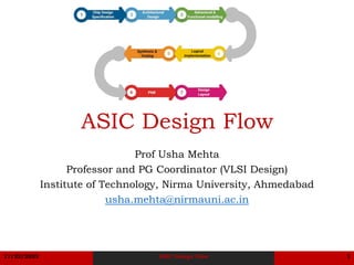
  • 1. 11/22/2023 ASIC Design Flow 1 ASIC Design Flow Prof Usha Mehta Professor and PG Coordinator (VLSI Design) Institute of Technology, Nirma University, Ahmedabad usha.mehta@nirmauni.ac.in
  • 2. 11/22/2023 ASIC Design Flow 2 Acknowledgement…. • This presentation has been summarized from various books, papers, websites and presentations related to the topic all over the world. I couldn’t remember where these large pull of hints and work come from. However, I’d like to thank all professors and scientists who created such a good work on this emerging field. Without those efforts in this very emerging technology, these notes and slides can’t be finished.
  • 3. 11/22/2023 ASIC Design Flow 3 Basic ASIC Design Flow
  • 5. 11/22/2023 ASIC Design Flow 5 • The above basic design flow is somehow over simplified in the sense that it only connects the design tasks in one direction. • Interactions between different stages, especially the influences of later stages on earlier ones, are not shown. • In reality, a design cannot be done in such a singular path. – If the timing analysis finds that the delay of the critical path is longer than that required by a clock period, we have to go back to the physical design to modify the layout. – If the problem cannot be resolved inside the physical design stage we then have to go back further to the circuit design to add buffers. – If we cannot resolve the problem through the modification of physical or circuit design, we would have to go back another stage to change the architecture design.
  • 6. 11/22/2023 ASIC Design Flow 6 • Most interference between different design stages is actually due to system performance requirements and variable remitting solutions at different stages. – As a consequence, we need to have loops in the design flow. • In general we want to go backward as little as possible. – A subsequent problem is that we might be end up cycling through these stages endlessly. – This issue is called timing closure
  • 7. 11/22/2023 ASIC Design Flow 7 Timing Closure
  • 8. 11/22/2023 ASIC Design Flow 8 Verification and Testing
  • 9. 11/22/2023 ASIC Design Flow 9 System Specification • A real ASIC design practice starts from understanding the application and writing a clear and complete specification in terms of VLSI terminology, such as input/output signals, clock rate, protocol definition, operation mode and etc. • Writing a specification for an ASIC project includes – Understanding the application – Communicating with customer for whom ASIC chip is designed – Converting application terminology into circuit design terminology – Defining system settings – Listing the performance criteria, and – Selecting the process
  • 10. 11/22/2023 ASIC Design Flow 10 Architectural Design • Architecture design • Architecture probably plays the most important role in determining the quality of a designed chip. • Experience in IC design and insight into the application contribute to the architecture choice. • Currently, architecture design still depends on the wisdom of the designer instead of on CAD tools, since there are too many factors involved. • Unfortunately the influence of different factors usually conflicts with each other. • Decisions on the architecture, e.g., RISC/CISC, # of ALU’s, pipeline structure, cache size, etc. Such decisions can provide an accurate estimation of the system performance, die size, power consumption, etc.
  • 11. 11/22/2023 ASIC Design Flow 11 Functional/Behavioural Design • Identify main functional units and their interconnections. No details of implementation. • Functional design is generally done with HDL
  • 12. 11/22/2023 ASIC Design Flow 12 Register Transfer Level + + 0010 0001 0100 0011 • Components, data types • Design the logic, e.g., Boolean expressions, control flow, word width, register allocation, etc. • RTL is expressed in a HDL mostly synthesized from behavioral description
  • 13. 11/22/2023 ASIC Design Flow 13 Logic Level • Discrete Level, Discrete Time • Design the circuit including gates, transistors, interconnections, etc. The outcome is called a netlist. • Homework ISCAS Gate level Netlist
  • 14. 11/22/2023 ASIC Design Flow 14 Circuit level • Continuous Voltage, Continuous time
  • 15. 11/22/2023 ASIC Design Flow 15 Layout • Convert the netlist into a geometric representation. The outcome is called a layout.
  • 16. 11/22/2023 ASIC Design Flow 16 Few more words… • Circuit Partitioning – Partition a large circuit into sub- circuits (called blocks). Factors like #blocks, block sizes, interconnection between blocks, etc., are considered. • Floorplanning – Set up a plan for a good layout. Place the modules (modules can be blocks, functional units, etc.) at an early stage when details like shape, area, I/O pin positions of the modules, …, are not yet fixed. • Placement – Exact placement of the modules (modules can be gates, standard cells, etc.) when details of the module design are known. The goal is to minimize the delay, total area and interconnect cost.
  • 17. 11/22/2023 ASIC Design Flow 17 • Routing – Complete the interconnections between modules. Factors like critical path, clock skew, wire spacing, etc., are considered. Include global routing and detailed routing. • Compaction – Compress the layout from all directions to minimize the total chip area. • Verification – Check the correctness of the layout. Include DRC (Design Rule Checking), circuit extraction (generate a circuit from the layout to compare with the original netlist), performance verification (extract geometric information to compute resistance, capacitance, delay, etc.)
  • 18. 11/22/2023 ASIC Design Flow 18 Cont…. • Logic Synthesizer • Translation from RTL specification to netlist • Adequate for the design that do not have critical performance parameter • Provides room to make design improvement • Understanding of device architecture is necessary • Gate Level Simulation • To ensure correctness of synthesis translation • Vendor supplied parameters are used to simulate the actual target device parameters
  • 19. 11/22/2023 ASIC Design Flow 19 Cont… • Extraction • Actual resistance and capacitance figures modelled for interconnections are extracted to simulate timing performance • Post Layout Simulation • Functionality taking care of timings • Time extraction imported • Both gate and interconnection delays are considered • Back Annotation • To update the initial circuit data with information that was obtained later in the design cycle • Passing the information related to the extra load that may occur in practice
  • 20. 11/22/2023 ASIC Design Flow 20 Cont… • Extended Testing • For ASIC, GA, SoG. • Not for FPGA • Device Programming • Via JTAG port • For FPGA
  • 21. 11/22/2023 ASIC Design Flow 21 VLSI Design Tools • By Chip vendor • By third party • Cadence • Mentor Graphics • Synopsis • Microwind
  • 23. 11/22/2023 ASIC Design Flow 23 Coverage of my area…. • ASIC • Full Custom • CMOS Design • Simulation • Layout • SemiCustom • Verification • Gate Array • Std. Cell • DFT • STA • FP-Floor Plan • CTC – Clock Tree Synthesis • FPGA • HDL Entry • Place and Route
  • 24. 11/22/2023 ASIC Design Flow 24 Thank you!