BCD-to-7 Segment Drivers
•
0 likes•64 views

DATASHEET

Recommended
More Related Content
What's hot
What's hot (19)
Similar to BCD-to-7 Segment Drivers
More from LITS IT Ltd,LASRC.SPACE,SAWDAGOR BD,FREELANCE BD,iREV,BD LAW ACADEMY,SMART AVI,HEA,HFSAC LTD.
More from LITS IT Ltd,LASRC.SPACE,SAWDAGOR BD,FREELANCE BD,iREV,BD LAW ACADEMY,SMART AVI,HEA,HFSAC LTD. (20)
Recently uploaded
Recently uploaded (20)
BCD-to-7 Segment Drivers
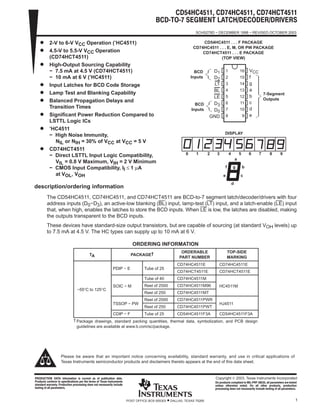
- 1. CD54HC4511, CD74HC4511, CD74HCT4511 BCDĆTOĆ7 SEGMENT LATCH/DECODER/DRIVERS SCHS279D − DECEMBER 1998 − REVISED OCTOBER 2003 1POST OFFICE BOX 655303 • DALLAS, TEXAS 75265 D 2-V to 6-V VCC Operation (’HC4511) D 4.5-V to 5.5-V VCC Operation (CD74HCT4511) D High-Output Sourcing Capability − 7.5 mA at 4.5 V (CD74HCT4511) − 10 mA at 6 V (’HC4511) D Input Latches for BCD Code Storage D Lamp Test and Blanking Capability D Balanced Propagation Delays and Transition Times D Significant Power Reduction Compared to LSTTL Logic ICs D ’HC4511 − High Noise Immunity, NIL or NIH = 30% of VCC at VCC = 5 V D CD74HCT4511 − Direct LSTTL Input Logic Compatibility, VIL = 0.8 V Maximum, VIH = 2 V Minimum − CMOS Input Compatibility, II ≤ 1 µA at VOL, VOH description/ordering information The CD54HC4511, CD74HC4511, and CD74HCT4511 are BCD-to-7 segment latch/decoder/drivers with four address inputs (D0−D3), an active-low blanking (BL) input, lamp-test (LT) input, and a latch-enable (LE) input that, when high, enables the latches to store the BCD inputs. When LE is low, the latches are disabled, making the outputs transparent to the BCD inputs. These devices have standard-size output transistors, but are capable of sourcing (at standard VOH levels) up to 7.5 mA at 4.5 V. The HC types can supply up to 10 mA at 6 V. ORDERING INFORMATION TA PACKAGE† ORDERABLE PART NUMBER TOP-SIDE MARKING PDIP − E Tube of 25 CD74HC4511E CD74HC4511E PDIP − E Tube of 25 CD74HCT4511E CD74HCT4511E Tube of 40 CD74HC4511M −55°C to 125°C SOIC − M Reel of 2500 CD74HC4511M96 HC4511M −55°C to 125°C SOIC − M Reel of 250 CD74HC4511MT HC4511M TSSOP − PW Reel of 2000 CD74HC4511PWR HJ4511TSSOP − PW Reel of 250 CD74HC4511PWT HJ4511 CDIP − F Tube of 25 CD54HC4511F3A CD54HC4511F3A † Package drawings, standard packing quantities, thermal data, symbolization, and PCB design guidelines are available at www.ti.com/sc/package. Copyright 2003, Texas Instruments IncorporatedPRODUCTION DATA information is current as of publication date. Products conform to specifications per the terms of Texas Instruments standard warranty. Production processing does not necessarily include testing of all parameters. Please be aware that an important notice concerning availability, standard warranty, and use in critical applications of Texas Instruments semiconductor products and disclaimers thereto appears at the end of this data sheet. 1 2 3 4 5 6 7 8 16 15 14 13 12 11 10 9 D1 D2 LT BL LE D3 D0 GND VCC f g a b c d e BCD Inputs BCD Inputs 7-Segment Outputs CD54HC4511 . . . F PACKAGE CD74HC4511 . . . E, M, OR PW PACKAGE CD74HCT4511 . . . E PACKAGE (TOP VIEW) 0 1 2 3 4 5 6 7 8 9 DISPLAY a b c d e f g On products compliant to MILĆPRFĆ38535, all parameters are tested unless otherwise noted. On all other products, production processing does not necessarily include testing of all parameters.
- 2. CD54HC4511, CD74HC4511, CD74HCT4511 BCDĆTOĆ7 SEGMENT LATCH/DECODER/DRIVERS SCHS279D − DECEMBER 1998 − REVISED OCTOBER 2003 2 POST OFFICE BOX 655303 • DALLAS, TEXAS 75265 FUNCTION TABLE INPUTS OUTPUTS LE BL LT D3 D2 D1 D0 a b c d e f g DISPLAY X X L X X X X H H H H H H H 8 X L H X X X X L L L L L L L Blank L H H L L L L H H H H H H L 0 L H H L L L H L H H L L L L 1 L H H L L H L H H L H H L H 2 L H H L L H H H H H H L L H 3 L H H L H L L L H H L L H H 4 L H H L H L H H L H H L H H 5 L H H L H H L L L H H H H H 6 L H H L H H H H H H L L L L 7 L H H H L L L H H H H H H H 8 L H H H L L H H H H L L H H 9 L H H H L H L L L L L L L L Blank L H H H L H H L L L L L L L Blank L H H H H L L L L L L L L L Blank L H H H H L H L L L L L L L Blank L H H H H H L L L L L L L L Blank L H H H H H H L L L L L L L Blank H H H X X X X † † † † † † † † X = Don’t care † Depends on BCD code previously applied when LE = L NOTE: Display is blank for all illegal input codes (BCD > HLLH). function diagram 7 1 2 6 5 4 D0 D1 D2 D3 LE BL LT 3 VSS = 8 VDD = 16 13 12 11 10 9 15 14 a b c d e f g Latch Decoder Driver 7-Segment Outputs BCD Inputs
- 3. CD54HC4511, CD74HC4511, CD74HCT4511 BCDĆTOĆ7 SEGMENT LATCH/DECODER/DRIVERS SCHS279D − DECEMBER 1998 − REVISED OCTOBER 2003 3POST OFFICE BOX 655303 • DALLAS, TEXAS 75265 logic diagram 15 f BL 4 6 2 1 7 5 14 9 11 12 13 a b c e g 3 LT D3 D2 D1 D0 LE LE LE LE LE LE LE LE LE LE LE LE LE LE LE LE LE D D D D Q Q Q Q Q Q Q Q Latch Latch Latch Latch LE LE 10 d
- 4. CD54HC4511, CD74HC4511, CD74HCT4511 BCDĆTOĆ7 SEGMENT LATCH/DECODER/DRIVERS SCHS279D − DECEMBER 1998 − REVISED OCTOBER 2003 4 POST OFFICE BOX 655303 • DALLAS, TEXAS 75265 absolute maximum ratings over operating free-air temperature (unless otherwise noted)† Supply voltage range, VCC −0.5 V to 7 V. . . . . . . . . . . . . . . . . . . . . . . . . . . . . . . . . . . . . . . . . . . . . . . . . . . . . . . . . . Input diode current, IIK (VI < −0.5 V or VI > VCC + 0.5 V) ) (see Note 1) ±20 mA. . . . . . . . . . . . . . . . . . . . . . . . Output diode current, IOK (VO < −0.5 V or VO > VCC + 0.5V) (see Note 1) ±20 mA. . . . . . . . . . . . . . . . . . . . . . Continuous output source or sink current per output, IO (VO = 0 to VCC) ±25 mA. . . . . . . . . . . . . . . . . . . . . . . Continuous current through VCC or GND ±50 mA. . . . . . . . . . . . . . . . . . . . . . . . . . . . . . . . . . . . . . . . . . . . . . . . . . . Package thermal impedance, θJA (see Note 2): E package 67°C/W. . . . . . . . . . . . . . . . . . . . . . . . . . . . . . . . . . . M package 73°C/W. . . . . . . . . . . . . . . . . . . . . . . . . . . . . . . . . . PW package 108°C/W. . . . . . . . . . . . . . . . . . . . . . . . . . . . . . . . Lead temperature (during soldering): At distance 1/16 ± 1/32 in (1.59 ± 0.79 mm) from case for 10 s maximum 265°C. . . . . . . . . . . . . . . . . . . . . Unit inserted into a PC board (minimum thickness 1/16 in, 1.59 mm), with solder contacting lead tips only 300°C. . . . . . . . . . . . . . . . . . . . . . . . . . . . . . . . . . . . . . . . . . . . . . . . . . . Storage temperature, Tstg −65 to 150°C. . . . . . . . . . . . . . . . . . . . . . . . . . . . . . . . . . . . . . . . . . . . . . . . . . . . . . . . . . . † Stresses beyond those listed under “absolute maximum ratings” may cause permanent damage to the device. These are stress ratings only, and functional operation of the device at these or any other conditions beyond those indicated under “recommended operating conditions” is not implied. Exposure to absolute-maximum-rated conditions for extended periods may affect device reliability. NOTES: 1. The input and output voltage ratings may be exceeded if the input and output current ratings are observed. 2. The package thermal impedance is calculated in accordance with JESD 51-7. recommended operating conditions for ’HC4511 (see Note 3) TA = 25°C TA = −55°C TO 125°C TA = −40°C TO 85°C UNIT MIN MAX MIN MAX MIN MAX UNIT VCC Supply voltage 2 6 2 6 2 6 V VCC = 2 V 1.5 1.5 1.5 VIH High-level input voltage VCC = 4.5 V 3.15 3.15 3.15 VVIH High-level input voltage VCC = 6 V 4.2 4.2 4.2 V VCC = 2 V 0.5 0.5 0.5 VIL Low-level input voltage VCC = 4.5 V 1.35 1.35 1.35 VVIL Low-level input voltage VCC = 6 V 1.8 1.8 1.8 V VI Input voltage 0 VCC 0 VCC 0 VCC V VO Output voltage 0 VCC 0 VCC 0 VCC V VCC = 2 V 1000 1000 1000 tt Input transition (rise and fall) time VCC = 4.5 V 500 500 500 nstt Input transition (rise and fall) time VCC = 6 V 400 400 400 ns NOTE 3: All unused inputs of the device must be held at VCC or GND to ensure proper device operation. Refer to the TI application report, Implications of Slow or Floating CMOS Inputs, literature number SCBA004.
- 5. CD54HC4511, CD74HC4511, CD74HCT4511 BCDĆTOĆ7 SEGMENT LATCH/DECODER/DRIVERS SCHS279D − DECEMBER 1998 − REVISED OCTOBER 2003 5POST OFFICE BOX 655303 • DALLAS, TEXAS 75265 recommended operating conditions for CD74HCT4511 (see Note 4) TA = 25°C TA = −55°C TO 125°C TA = −40°C TO 85°C UNIT MIN MAX MIN MAX MIN MAX UNIT VCC Supply voltage 4.5 5.5 4.5 5.5 4.5 5.5 V VIH High-level input voltage 2 2 2 V VIL Low-level input voltage 0.8 0.8 0.8 V VI Input voltage VCC VCC VCC V VO Output voltage VCC VCC VCC V tt Input transition (rise and fall) time 500 500 500 ns NOTE 4: All unused inputs of the device must be held at VCC or GND to ensure proper device operation. Refer to the TI application report, Implications of Slow or Floating CMOS Inputs, literature number SCBA004. ’HC4511 electrical characteristics over recommended operating free-air temperature range (unless otherwise noted) PARAMETER TEST CONDITIONS VCC TA = 25°C TA = −55°C TO 125°C TA = −40°C TO 85°C UNITPARAMETER TEST CONDITIONS VCC MIN MAX MIN MAX MIN MAX UNIT 2 V 1.9 1.9 1.9 IOH = −20 µA 4.5 V 4.4 4.4 4.4 VOH VI = VIH or VIL IOH = −20 µA 6 V 5.9 5.9 5.9 VVOH VI = VIH or VIL IOH = −7.5 mA 4.5 V 3.98 3.7 3.84 V IOH = −10 mA 6 V 5.48 5.2 5.34 2 V 0.1 0.1 0.1 IOL = 20 µA 4.5 V 0.1 0.1 0.1 VOL VI = VIH or VIL IOL = 20 µA 6 V 0.1 0.1 0.1 VVOL VI = VIH or VIL IOL = 4 mA 4.5 V 0.26 0.4 0.33 V IOL = 5.2 mA 6 V 0.26 0.4 0.33 II VI = VCC or 0 6 V ±0.1 ±1 ±1 µA ICC VI = VCC or 0, IO = 0 6 V 8 160 80 µA Ci 10 10 10 pF
- 6. CD54HC4511, CD74HC4511, CD74HCT4511 BCDĆTOĆ7 SEGMENT LATCH/DECODER/DRIVERS SCHS279D − DECEMBER 1998 − REVISED OCTOBER 2003 6 POST OFFICE BOX 655303 • DALLAS, TEXAS 75265 CD74HCT4511 electrical characteristics over recommended operating free-air temperature range (unless otherwise noted) PARAMETER TEST CONDITIONS VCC TA = 25°C TA = −55°C TO 125°C TA = −40°C TO 85°C UNITPARAMETER TEST CONDITIONS VCC MIN TYP MAX MIN MAX MIN MAX UNIT VOH VI = VIH or VIL IOH = −20 µA 4.5 V 4.4 4.4 4.4 VVOH VI = VIH or VIL IOH = −4 mA 4.5 V 3.98 3.7 3.84 V VOL VI = VIH or VIL IOL = 20 µA 4.5 V 0.1 0.1 0.1 VVOL VI = VIH or VIL IOL = 4 mA 4.5 V 0.26 0.4 0.33 V II VI = VCC to GND 5.5 V ±0.1 ±1 ±1 µA ICC VI = VCC or 0, IO = 0 5.5 V 8 160 80 µA ∆ICC† One input at VCC − 2.1 V, Other inputs at 0 or VCC 4.5 V to 5.5 V 100 360 490 450 µA Ci 10 10 10 pF † Additional quiescent supply current per input pin, TTL inputs high, 1 unit load. For dual-supply systems, theoretical worst-case (VI = 2.4 V, VCC = 5.5 V) specification is 1.8 mA. HCT INPUT LOADING TABLE INPUT UNIT LOADS‡ LT, LE 1.5 BL, Dn 0.3 ‡ Unit load is ∆ICC limit specified in electrical characteristics table, e.g., 360 µA maximum at 25°C. ’HC4511 timing requirements over recommended operating free-air temperature range (unless otherwise noted) (see Figure 1) VCC TA = 25°C TA = −55°C TO 125°C TA = −40°C TO 85°C UNITVCC MIN MAX MIN MAX MIN MAX UNIT 2 V 80 120 100 tw Pulse duration, LE low 4.5 V 16 24 20 nstw Pulse duration, LE low 6 V 14 20 17 ns 2 V 60 90 75 tsu Setup time, BCD inputs before LE↑ 4.5 V 12 18 15 nstsu Setup time, BCD inputs before LE↑ 6 V 10 15 13 ns 2 V 3 3 3 th Hold time, BCD inputs before LE↑ 4.5 V 3 3 3 nsth Hold time, BCD inputs before LE↑ 6 V 3 3 3 ns
- 7. CD54HC4511, CD74HC4511, CD74HCT4511 BCDĆTOĆ7 SEGMENT LATCH/DECODER/DRIVERS SCHS279D − DECEMBER 1998 − REVISED OCTOBER 2003 7POST OFFICE BOX 655303 • DALLAS, TEXAS 75265 ’HC4511 switching characteristics over recommended operating free-air temperature range (unless otherwise noted) (see Figure 1) PARAMETER FROM (INPUT) TO (OUTPUT) LOAD CAPACITANCE VCC TA = 25°C TA = −55°C TO 125°C TA = −40°C TO 85°C UNITPARAMETER (INPUT) (OUTPUT) CAPACITANCE VCC MIN TYP MAX MIN MAX MIN MAX UNIT 2 V 300 450 375 Dn Output CL = 50 pF 4.5 V 60 90 75 Dn Output CL = 50 pF 6 V 51 77 64 CL = 15 pF 5 V 25 2 V 270 405 340 LE Output CL = 50 pF 4.5 V 54 81 68 LE Output CL = 50 pF 6 V 46 69 58 tpd CL = 15 pF 5 V 23 nstpd 2 V 220 330 275 ns BL Output CL = 50 pF 4.5 V 44 66 55 BL Output CL = 50 pF 6 V 37 56 47 CL = 15 pF 5 V 18 2 V 160 240 200 LT Output CL = 50 pF 4.5 V 32 48 40 LT Output CL = 50 pF 6 V 27 41 34 CL = 15 pF 5 V 13 2 V 75 110 95 tt Any CL = 50 pF 4.5 V 15 22 19 nstt Any CL = 50 pF 6 V 13 19 16 ns
- 8. CD54HC4511, CD74HC4511, CD74HCT4511 BCDĆTOĆ7 SEGMENT LATCH/DECODER/DRIVERS SCHS279D − DECEMBER 1998 − REVISED OCTOBER 2003 8 POST OFFICE BOX 655303 • DALLAS, TEXAS 75265 CD74HCT4511 timing requirements over recommended operating free-air temperature range VCC = 4.5 V (unless otherwise noted) (see Figure 2) TA = 25°C TA = −55°C TO 125°C TA = −40°C TO 85°C UNIT MIN MAX MIN MAX MIN MAX UNIT tw Pulse duration, LE low 16 24 20 ns tsu Setup time, BCD inputs before LE↑ 16 24 20 ns th Hold time, BCD inputs before LE↑ 5 5 5 ns CD74HCT4511 switching characteristics over recommended operating free-air temperature range (unless otherwise noted) (see Figure 2) PARAMETER FROM (INPUT) TO (OUTPUT) LOAD CAPACITANCE VCC TA = 25°C TA = −55°C TO 125°C TA = −40°C TO 85°C UNITPARAMETER (INPUT) (OUTPUT) CAPACITANCE VCC MIN TYP MAX MIN MAX MIN MAX UNIT Dn Output CL = 50 pF 4.5 V 60 90 75 Dn Output CL = 15 pF 5 V 25 LE Output CL = 50 pF 4.5 V 54 81 68 tpd LE Output CL = 15 pF 5 V 23 nstpd BL Output CL = 50 pF 4.5 V 44 66 55 ns BL Output CL = 15 pF 5 V 18 LT Output CL = 50 pF 4.5 V 33 50 41 LT Output CL = 15 pF 5 V 13 tt Any CL = 50 pF 4.5 V 15 22 19 ns operating characteristics, VCC = 5 V, TA = 25°C PARAMETER TYP UNIT Cpd† Power dissipation capacitance ’HC4511 114 pFCpd† Power dissipation capacitance CD74HCT4511 110 pF † Cpd is used to determine the dynamic power consumption, per package. PD = Cpd VCC2 fi + ∑ CL VCC2 fo where: fi = input frequency fo = output frequency CL = output load capacitance VCC = supply voltage
- 9. CD54HC4511, CD74HC4511, CD74HCT4511 BCDĆTOĆ7 SEGMENT LATCH/DECODER/DRIVERS SCHS279D − DECEMBER 1998 − REVISED OCTOBER 2003 9POST OFFICE BOX 655303 • DALLAS, TEXAS 75265 PARAMETER MEASUREMENT INFORMATION − ’HC4511 Test Point From Output Under Test CL (see Note A) VCC S1 S2 LOAD CIRCUIT PARAMETER tPZH tpd or tt tdis ten tPZL tPHZ tPLZ Open Closed S1 Closed Open S2 Open Closed Closed Open Open Open NOTES: A. CL includes probe and test-fixture capacitance. B. Waveform 1 is for an output with internal conditions such that the output is low except when disabled by the output control. Waveform 2 is for an output with internal conditions such that the output is high except when disabled by the output control. C. Phase relationships between waveforms were chosen arbitrarily. All input pulses are supplied by generators having the following characteristics: PRR ≤ 1 MHz, ZO = 50 Ω, tr = 6 ns, tf = 6 ns. D. For clock inputs, fmax is measured with the input duty cycle at 50%. E. The outputs are measured one at a time with one input transition per measurement. F. tPLZ and tPHZ are the same as tdis. G. tPZL and tPZH are the same as ten. H. tPLH and tPHL are the same as tpd. RL = 1 kΩ VOLTAGE WAVEFORMS SETUP AND HOLD AND INPUT RISE AND FALL TIMES thtsu 50% VCC 50% VCC50% 10%10% 90% 90% VCC VCC 0 V 0 V tr tf Reference Input Data Input VOLTAGE WAVEFORMS PROPAGATION DELAY AND OUTPUT TRANSITION TIMES 50% VCC 50% VCC50% 10%10% 90% 90% VCC VOH VOL 0 V tr tf Input In-Phase Output 50% VCC tPLH tPHL 50% VCC 50% 10% 10% 90%90% VOH VOL trtf tPHL tPLH Out-of-Phase Output 0 V tw VOLTAGE WAVEFORMS PULSE DURATION Input 50% VCC50% VCC VCC Output Control Output Waveform 1 (see Note B) Output Waveform 2 (see Note B) VOL VOH tPZL tPZH tPLZ tPHZ ≈VCC 0 V 50% VCC 10% 50% VCC ≈0 V VOLTAGE WAVEFORMS OUTPUT ENABLE AND DISABLE TIMES 50% VCC 50% VCC 90% VCC VOLTAGE WAVEFORMS RECOVERY TIME 50% VCC VCC 0 V CLR Input CLK 50% VCC VCC trec 0 V Figure 1. Load Circuit and Voltage Waveforms
- 10. CD54HC4511, CD74HC4511, CD74HCT4511 BCDĆTOĆ7 SEGMENT LATCH/DECODER/DRIVERS SCHS279D − DECEMBER 1998 − REVISED OCTOBER 2003 10 POST OFFICE BOX 655303 • DALLAS, TEXAS 75265 PARAMETER MEASUREMENT INFORMATION − CD74HCT4511 Test Point From Output Under Test CL (see Note A) VCC S1 S2 LOAD CIRCUIT PARAMETER tPZH tpd or tt tdis ten tPZL tPHZ tPLZ Open Closed S1 Closed Open S2 Open Closed Closed Open Open Open NOTES: A. CL includes probe and test-fixture capacitance. B. Waveform 1 is for an output with internal conditions such that the output is low except when disabled by the output control. Waveform 2 is for an output with internal conditions such that the output is high except when disabled by the output control. C. Phase relationships between waveforms were chosen arbitrarily. All input pulses are supplied by generators having the following characteristics: PRR ≤ 1 MHz, ZO = 50 Ω, tr = 6 ns, tf = 6 ns. D. For clock inputs, fmax is measured with the input duty cycle at 50%. E. The outputs are measured one at a time with one input transition per measurement. F. tPLZ and tPHZ are the same as tdis. G. tPZL and tPZH are the same as ten. H. tPLH and tPHL are the same as tpd. RL = 1 kΩ VOLTAGE WAVEFORMS SETUP AND HOLD AND INPUT RISE AND FALL TIMES thtsu 50% VCC 50% VCC50% 10%10% 90% 90% VCC VCC 0 V 0 V tr tf Reference Input Data Input VOLTAGE WAVEFORMS PROPAGATION DELAY AND OUTPUT TRANSITION TIMES 50% VCC 50% VCC50% 10%10% 90% 90% VCC VOH VOL 0 V tr tf Input In-Phase Output 50% VCC tPLH tPHL 50% VCC 50% 10% 10% 90%90% VOH VOL trtf tPHL tPLH Out-of-Phase Output 0 V tw VOLTAGE WAVEFORMS PULSE DURATION Input 50% VCC50% VCC VCC Output Control Output Waveform 1 (see Note B) Output Waveform 2 (see Note B) VOL VOH tPZL tPZH tPLZ tPHZ ≈VCC 0 V 50% VCC 10% 50% VCC ≈0 V VOLTAGE WAVEFORMS OUTPUT ENABLE AND DISABLE TIMES 50% VCC 50% VCC 90% VCC VOLTAGE WAVEFORMS RECOVERY TIME 50% VCC VCC 0 V CLR Input CLK 50% VCC VCC trec 0 V Figure 2. Load Circuit and Voltage Waveforms
- 11. PACKAGE OPTION ADDENDUM www.ti.com 28-Jul-2020 Addendum-Page 1 PACKAGING INFORMATION Orderable Device Status (1) Package Type Package Drawing Pins Package Qty Eco Plan (2) Lead finish/ Ball material (6) MSL Peak Temp (3) Op Temp (°C) Device Marking (4/5) Samples 5962-8773301EA ACTIVE CDIP J 16 1 TBD SNPB N / A for Pkg Type -55 to 125 5962-8773301EA CD54HC4511F3A CD54HC4511F3A ACTIVE CDIP J 16 1 TBD SNPB N / A for Pkg Type -55 to 125 5962-8773301EA CD54HC4511F3A CD74HC4511E ACTIVE PDIP N 16 25 Green (RoHS & no Sb/Br) NIPDAU N / A for Pkg Type -55 to 125 CD74HC4511E CD74HC4511EE4 ACTIVE PDIP N 16 25 Green (RoHS & no Sb/Br) NIPDAU N / A for Pkg Type -55 to 125 CD74HC4511E CD74HC4511M ACTIVE SOIC D 16 40 Green (RoHS & no Sb/Br) NIPDAU Level-1-260C-UNLIM -55 to 125 HC4511M CD74HC4511M96 ACTIVE SOIC D 16 2500 Green (RoHS & no Sb/Br) NIPDAU Level-1-260C-UNLIM -55 to 125 HC4511M CD74HC4511M96E4 ACTIVE SOIC D 16 2500 Green (RoHS & no Sb/Br) NIPDAU Level-1-260C-UNLIM -55 to 125 HC4511M CD74HC4511MG4 ACTIVE SOIC D 16 40 Green (RoHS & no Sb/Br) NIPDAU Level-1-260C-UNLIM -55 to 125 HC4511M CD74HC4511MT ACTIVE SOIC D 16 250 Green (RoHS & no Sb/Br) NIPDAU Level-1-260C-UNLIM -55 to 125 HC4511M CD74HC4511PWR ACTIVE TSSOP PW 16 2000 Green (RoHS & no Sb/Br) NIPDAU Level-1-260C-UNLIM -55 to 125 HJ4511 CD74HC4511PWRE4 ACTIVE TSSOP PW 16 2000 Green (RoHS & no Sb/Br) NIPDAU Level-1-260C-UNLIM -55 to 125 HJ4511 CD74HC4511PWRG4 ACTIVE TSSOP PW 16 2000 Green (RoHS & no Sb/Br) NIPDAU Level-1-260C-UNLIM -55 to 125 HJ4511 CD74HC4511PWT ACTIVE TSSOP PW 16 250 Green (RoHS & no Sb/Br) NIPDAU Level-1-260C-UNLIM -55 to 125 HJ4511 CD74HC4511PWTE4 ACTIVE TSSOP PW 16 250 Green (RoHS & no Sb/Br) NIPDAU Level-1-260C-UNLIM -55 to 125 HJ4511 CD74HCT4511E ACTIVE PDIP N 16 25 Green (RoHS & no Sb/Br) NIPDAU N / A for Pkg Type -55 to 125 CD74HCT4511E CD74HCT4511EE4 ACTIVE PDIP N 16 25 Green (RoHS & no Sb/Br) NIPDAU N / A for Pkg Type -55 to 125 CD74HCT4511E (1) The marketing status values are defined as follows:
- 12. PACKAGE OPTION ADDENDUM www.ti.com 28-Jul-2020 Addendum-Page 2 ACTIVE: Product device recommended for new designs. LIFEBUY: TI has announced that the device will be discontinued, and a lifetime-buy period is in effect. NRND: Not recommended for new designs. Device is in production to support existing customers, but TI does not recommend using this part in a new design. PREVIEW: Device has been announced but is not in production. Samples may or may not be available. OBSOLETE: TI has discontinued the production of the device. (2) RoHS: TI defines "RoHS" to mean semiconductor products that are compliant with the current EU RoHS requirements for all 10 RoHS substances, including the requirement that RoHS substance do not exceed 0.1% by weight in homogeneous materials. Where designed to be soldered at high temperatures, "RoHS" products are suitable for use in specified lead-free processes. TI may reference these types of products as "Pb-Free". RoHS Exempt: TI defines "RoHS Exempt" to mean products that contain lead but are compliant with EU RoHS pursuant to a specific EU RoHS exemption. Green: TI defines "Green" to mean the content of Chlorine (Cl) and Bromine (Br) based flame retardants meet JS709B low halogen requirements of <=1000ppm threshold. Antimony trioxide based flame retardants must also meet the <=1000ppm threshold requirement. (3) MSL, Peak Temp. - The Moisture Sensitivity Level rating according to the JEDEC industry standard classifications, and peak solder temperature. (4) There may be additional marking, which relates to the logo, the lot trace code information, or the environmental category on the device. (5) Multiple Device Markings will be inside parentheses. Only one Device Marking contained in parentheses and separated by a "~" will appear on a device. If a line is indented then it is a continuation of the previous line and the two combined represent the entire Device Marking for that device. (6) Lead finish/Ball material - Orderable Devices may have multiple material finish options. Finish options are separated by a vertical ruled line. Lead finish/Ball material values may wrap to two lines if the finish value exceeds the maximum column width. Important Information and Disclaimer:The information provided on this page represents TI's knowledge and belief as of the date that it is provided. TI bases its knowledge and belief on information provided by third parties, and makes no representation or warranty as to the accuracy of such information. Efforts are underway to better integrate information from third parties. TI has taken and continues to take reasonable steps to provide representative and accurate information but may not have conducted destructive testing or chemical analysis on incoming materials and chemicals. TI and TI suppliers consider certain information to be proprietary, and thus CAS numbers and other limited information may not be available for release. In no event shall TI's liability arising out of such information exceed the total purchase price of the TI part(s) at issue in this document sold by TI to Customer on an annual basis. OTHER QUALIFIED VERSIONS OF CD54HC4511, CD74HC4511 : •Catalog: CD74HC4511 •Military: CD54HC4511 NOTE: Qualified Version Definitions: •Catalog - TI's standard catalog product
- 13. PACKAGE OPTION ADDENDUM www.ti.com 28-Jul-2020 Addendum-Page 3 •Military - QML certified for Military and Defense Applications
- 14. TAPE AND REEL INFORMATION *All dimensions are nominal Device Package Type Package Drawing Pins SPQ Reel Diameter (mm) Reel Width W1 (mm) A0 (mm) B0 (mm) K0 (mm) P1 (mm) W (mm) Pin1 Quadrant CD74HC4511M96 SOIC D 16 2500 330.0 16.4 6.5 10.3 2.1 8.0 16.0 Q1 CD74HC4511PWR TSSOP PW 16 2000 330.0 12.4 6.9 5.6 1.6 8.0 12.0 Q1 CD74HC4511PWT TSSOP PW 16 250 330.0 12.4 6.9 5.6 1.6 8.0 12.0 Q1 PACKAGE MATERIALS INFORMATION www.ti.com 19-Oct-2020 Pack Materials-Page 1
- 15. *All dimensions are nominal Device Package Type Package Drawing Pins SPQ Length (mm) Width (mm) Height (mm) CD74HC4511M96 SOIC D 16 2500 333.2 345.9 28.6 CD74HC4511PWR TSSOP PW 16 2000 853.0 449.0 35.0 CD74HC4511PWT TSSOP PW 16 250 853.0 449.0 35.0 PACKAGE MATERIALS INFORMATION www.ti.com 19-Oct-2020 Pack Materials-Page 2
- 19. www.ti.com PACKAGE OUTLINE C 14X 0.65 2X 4.55 16X 0.30 0.19 TYP 6.6 6.2 1.2 MAX 0.15 0.05 0.25 GAGE PLANE -80 B NOTE 4 4.5 4.3 A NOTE 3 5.1 4.9 0.75 0.50 (0.15) TYP TSSOP - 1.2 mm max heightPW0016A SMALL OUTLINE PACKAGE 4220204/A 02/2017 1 8 9 16 0.1 C A B PIN 1 INDEX AREA SEE DETAIL A 0.1 C NOTES: 1. All linear dimensions are in millimeters. Any dimensions in parenthesis are for reference only. Dimensioning and tolerancing per ASME Y14.5M. 2. This drawing is subject to change without notice. 3. This dimension does not include mold flash, protrusions, or gate burrs. Mold flash, protrusions, or gate burrs shall not exceed 0.15 mm per side. 4. This dimension does not include interlead flash. Interlead flash shall not exceed 0.25 mm per side. 5. Reference JEDEC registration MO-153. SEATING PLANE A 20 DETAIL A TYPICAL SCALE 2.500
- 20. www.ti.com EXAMPLE BOARD LAYOUT 0.05 MAX ALL AROUND 0.05 MIN ALL AROUND 16X (1.5) 16X (0.45) 14X (0.65) (5.8) (R0.05) TYP TSSOP - 1.2 mm max heightPW0016A SMALL OUTLINE PACKAGE 4220204/A 02/2017 NOTES: (continued) 6. Publication IPC-7351 may have alternate designs. 7. Solder mask tolerances between and around signal pads can vary based on board fabrication site. LAND PATTERN EXAMPLE EXPOSED METAL SHOWN SCALE: 10X SYMM SYMM 1 8 9 16 15.000 METAL SOLDER MASK OPENING METAL UNDER SOLDER MASK SOLDER MASK OPENING EXPOSED METALEXPOSED METAL SOLDER MASK DETAILS NON-SOLDER MASK DEFINED (PREFERRED) SOLDER MASK DEFINED
- 21. www.ti.com EXAMPLE STENCIL DESIGN 16X (1.5) 16X (0.45) 14X (0.65) (5.8) (R0.05) TYP TSSOP - 1.2 mm max heightPW0016A SMALL OUTLINE PACKAGE 4220204/A 02/2017 NOTES: (continued) 8. Laser cutting apertures with trapezoidal walls and rounded corners may offer better paste release. IPC-7525 may have alternate design recommendations. 9. Board assembly site may have different recommendations for stencil design. SOLDER PASTE EXAMPLE BASED ON 0.125 mm THICK STENCIL SCALE: 10X SYMM SYMM 1 8 9 16
- 23. IMPORTANT NOTICE AND DISCLAIMER TI PROVIDES TECHNICAL AND RELIABILITY DATA (INCLUDING DATASHEETS), DESIGN RESOURCES (INCLUDING REFERENCE DESIGNS), APPLICATION OR OTHER DESIGN ADVICE, WEB TOOLS, SAFETY INFORMATION, AND OTHER RESOURCES “AS IS” AND WITH ALL FAULTS, AND DISCLAIMS ALL WARRANTIES, EXPRESS AND IMPLIED, INCLUDING WITHOUT LIMITATION ANY IMPLIED WARRANTIES OF MERCHANTABILITY, FITNESS FOR A PARTICULAR PURPOSE OR NON-INFRINGEMENT OF THIRD PARTY INTELLECTUAL PROPERTY RIGHTS. These resources are intended for skilled developers designing with TI products. You are solely responsible for (1) selecting the appropriate TI products for your application, (2) designing, validating and testing your application, and (3) ensuring your application meets applicable standards, and any other safety, security, or other requirements. These resources are subject to change without notice. TI grants you permission to use these resources only for development of an application that uses the TI products described in the resource. Other reproduction and display of these resources is prohibited. No license is granted to any other TI intellectual property right or to any third party intellectual property right. TI disclaims responsibility for, and you will fully indemnify TI and its representatives against, any claims, damages, costs, losses, and liabilities arising out of your use of these resources. TI’s products are provided subject to TI’s Terms of Sale (www.ti.com/legal/termsofsale.html) or other applicable terms available either on ti.com or provided in conjunction with such TI products. TI’s provision of these resources does not expand or otherwise alter TI’s applicable warranties or warranty disclaimers for TI products. Mailing Address: Texas Instruments, Post Office Box 655303, Dallas, Texas 75265 Copyright © 2020, Texas Instruments Incorporated