
Recommended
More Related Content
Similar to COA Chapter 1.pdf
Similar to COA Chapter 1.pdf (20)
Recently uploaded
Recently uploaded (20)
COA Chapter 1.pdf
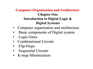
- 1. Computer Organization andArchitecture Chapter One Introduction to Digital Logic & Digital Systems 1 • Computer organization and architecture • Basic components of Digital system • Logic Gates • Combinational Circuits • Flip-Flops • Sequential Circuits • K-map Minimization
- 2. 2 ComputerArchitecture and Organization What is ComputerArchitecture? • It is concerned with behavior of various functional modules (HW and SW) of a digital computer as well as how these modules interact to meet the requirement of the user • Deals with interface between hardware and software • ComputerArchitecture helps us to understand the functionalities of a system. (deals with high-level design issues) Describes WHAT the computer does (logical view) • Examples: the instruction set (what operations can be performed?) the number of bits used to represent various data types methods used for input-output (I/O mechanism), etc.
- 3. 3 ComputerArchitecture and Organization Computer Organization • Deals with structural relationship. • It is concerned with ways in which the hardware components operate and the way they are interconnected together to form a computer system • Concerned with information flow between components and means by which such information flow is controlled • It covers the hardware units and their connection details • Describes how it does it (how does a computer work) • A computer's organization expresses the realization of the architecture or how the physical aspects of a computer systems are implemented. • Eg. Circuit design, Control Signals, Memory types, peripherals, etc
- 4. 4 ComputerArchitecture and Organization Computer Design: • Is concerned with the hardware design of the computer. • Once the computer specification is formulated, it is the task of the designer to develop hardware for the system. • While designing a computer architecture is considered first.An organization is done on the basis of architecture.
- 5. Basic Components of Computer • The digital computer is a digital system that performs various computational tasks. • Computer is made up of the following HW components: – ACentral Processing Unit • Arithmetic & Logic Unit • Control Unit • Registers – Memory • any physical device capable of storing information temporarily or permanently – Primary Memory (Usually called RAM) – Secondary Memory or Mass Storage (Disk drives) – Input and Output Devices • allow the computer system to interact with the outside world by moving data into and out of the system. 5
- 6. Organization of the computer Block Diagram of a digital Computer - How computer work
- 7. Logic Gates • The building blocks used to create digital circuits are logic gates – Gates are used as the building blocks in the design of more complex digital logic circuits • There are three elementary logic gates and a range of other simple gates • Each gate has its own logic symbol which allows complex functions to be represented by a logic diagram • The function of each gate can be represented by a truth table or using Boolean notation
- 8. Logic Gates • The seven basic logic gates includes:AND, OR, NOT, NAND, NOR, XOR, and XNOR. 1. The AND gate
- 9. Logic Gates 2. The OR gate
- 10. Logic Gates 3. The NOT gate (or inverter)
- 11. Logic Gates 4. The NAND gate – Is the complement of AND gate
- 12. Logic Gates 5. The NOR gate – Is the complement of OR gate
- 13. Logic Gates 6. The Exclusive OR gate C=A’B+AB’
- 14. Logic Gates 7. The Exclusive NOR gate
- 15. Boolean Algebra - Boolean Notation is a annotation that deals with binary variables and logic operations. - Variables are designated by letters such as A, B, x, and y. - The result of a Boolean function is either 0 or 1. Basic Identities of Boolean algebra (1) x + 0 = x (3) x + 1 = 1 (2) x * 1 = x (4) x * 0 = 0 (5) x + x = x (6) x * x = x (7) x + x' = 1 (8) x * x' = 0 (9) x + y = y + x (10) xy = yx (11) x + (y + z) = (x + y) + z (12) x(yz) = (xy)z (13) x(y + z) = xy + xz (14) x + yz = (x + y)(x + z) (15) (x + y)' = x'y' (16) (xy)' = x' + y‘ (17) (x')' = x (18) x(x+y)=x
- 16. Example 1
- 17. Logical Expression Simplification - Algebraic manipulation use Boolean laws to simplify the expression difficult to use. The map-method (K-map Simplification) – The map method provides a simple straight forward procedures for minimizing Boolean functions - The map method is known as the Karnaugh map or K-map. - Each combination of the variables in a truth table is called a min term. - There are 2n min terms for a function of n variables. - The Boolean algebra can simplify by those two methods: 1. Sum-of- Products simplifications (SOP) 2. Product-of-sum simplifications (POS)
- 18. Variable Maps
- 19. Sum-of-Products Simplification ((SOP) - A Boolean function represented by a truth table is plotted into the map by inserting 1's into those squares where the function is 1. - The objective to identify adjacent squares containing 1's and group them together. - Groups of combined adjacent squares may share one or more squares with one or more groups. - Each group of squares represents an algebraic term, and the OR of those terms gives the simplified algebraic expression for the function. - To find the most simplified algebraic expression, the goal of map simplification is to identify the least number of groups with the largest number of members. Example: We will simplify the Boolean function. F(A,B,C) = Σ(0,2,4,5,6)
- 20. Cont… Map for F(A,B,C) = Σ(0,2, 4, 5, 6) The simplified expressions of the function is : F = C’+AB’
- 21. Maps for F(A,B,C,D)=Σ(0,1,2,6,8,9,10) So the simplified function is: F = B’D’ + B’C’ + A’CD’
- 22. Product-of-Sums Simplification (POS) - This approach is similar to the Sum-of-Products simplification, but identifying adjacent squares containing 0’s instead of 1’s forms the groups of adjacent squares. - Then, instead of representing the function as a sum of products, the function is represented as a product of sums. - Examples: F(A,B,C,D) = 𝝅 (0,1,2,5,8,9,10)
- 23. POS Example • F(A,B,C)=π(4,5,3,2,6,7) POS of F=A’B’ NH Read about don’t care condition
- 24. Deriving Logical Expressions (cont.) • 3-input majority function A B C F 0 0 0 0 0 0 1 0 0 1 0 0 0 1 1 1 1 0 0 0 1 0 1 1 1 1 0 1 1 1 1 1 • SOP logical expression • Four product terms – -Because there are 4 rows with a 1 output F = A B C + A B C + A B C + A B C
- 25. Deriving Logical Expressions (cont.) • 3-input majority function A B C F 0 0 0 0 0 0 1 0 0 1 0 0 0 1 1 1 1 0 0 0 1 0 1 1 1 1 0 1 1 1 1 1 • POS logical expression • Four sum terms – Because there are 4 rows with a 0 output F = (A + B + C) (A + B + C) ( A + B + C) ( A + B + C)
- 26. Combinational Circuits • A combinational circuit is a connected arrangement of logic gates with a set of inputs and outputs. • The output is dependent upon combination of input variable. • The state of the output at any instant is entirely determined by the states of the inputs at that time. • Gates are basic combinational circuits themselves, and gates used to construct more complex combinational functions. • Combinational circuits are employed in digital computers: – For generating binary control decisions and – For providing digital components required for data processing
- 27. Combinational logic where the outputs are determined solely(only) by the current states of the inputs Examples • Adders (Half adder and Full adder) • Decoders /Encoders • Multiplexers/ Demultiplexers • Comparator Used to implement comparison operators (= , > , < , , )
- 28. Half-Adder • The most basic digital arithmetic circuit. • Performs the addition of two binary digits. • The input variables of a half-adder are called the augends • The output variables of a half-adder are called the sum (S) and the carry (C). half adder S = x’y+xy’=x ⊕ y C=xy
- 29. Full-Adder • Afull-adder performs the addition of three binary digits. • Two half-adders can be combined to form a full-adder. • Full adder has three inputs and two outputs • The full adder circuit contains two half adders and an OR gate.
- 30. Decoder • A decoder is a combinational circuit that converts binary information from the n coded inputs to a maximum of 2n unique outputs. • Consists of: n Inputs and 2n Outputs (numbered from 0 - 2n - 1) • The truth table of 3-to-8 Decoder is shown below:
- 31. Decoder Logic Diagram for 3-to-8 Decoder Decoders typically include one or more enable inputs to control (turn on/off) the operation of a circuit.
- 32. Multiplexer (MUX)/selector • It is a combinational circuit that receives input from one of 2n input data lines and directs it to a single output line. • The selection of a particular input data line for a particular output is determined by a set of selection inputs. • A2n-to-1 multiplexer has 2n input data lines and n input selection lines.
- 33. Multiplex ers • Multiplexer – 2n data inputs – n selection inputs – a single output • Selection input determines the input that should be connected to the output 4-data input MUX
- 34. Multiplexers • Like encoders, Multiplexers can have an enable input to control the operation of the unit. 4-to-1 multiplexer Function Table
- 35. Flip-Flops • It is a binary cell capable of storing just one bit of information (it contains 0 or 1) • Flip flops are the smallest temporary storage units /memory/of a computer • It is a bistable device (i.e. it has two stable states: its output remains either high (1) or low (0)) • The high state ,i.e, 1 is called Set and the low state, i.e, 0 is called the Reset or clear state
- 36. Flip-Flops All flip flops have two outputs, one for the normal value (Q) and other giving a value opposite to the value stored in the flip flop (Q’) Flip flops are of many types depending on the number of inputs they have and how these inputs affect the outputs. The most common types of flip flops are: • SR Flip- Flop • D Flip- Flop • JK Flip- Flop • T Flip- Flop
- 37. Flip-Flops • SR (set-reset) Flip- Flop – Can be constructed using two NOR gates – There are two inputs (S & R) and two outputs (Q & Q’) R S Q Q' S R Q 0 0 hold 0 1 0 1 0 1 1 1 disallow
- 38. Flip-Flops • SR Flip Flops R S Q Q S R Q0 Q Q’ 0 0 0 0 1 0 0 1 1 0 0 1 0 0 1 0 1 1 0 1 1 0 0 1 0 1 0 1 1 0 1 1 0 0 0 1 1 1 0 0 0 1 1 1 0 Q = 0 Q = Q0 Q = 1 Q = Q’ Q = Q’
- 39. Flip-Flops • SR Flip- Flop
- 40. Flip-Flops • Disadvantages of SR flip flop 1. It needs two data inputs a high S to store a 1 bit and a high R to store 0 bit • Generation of two signals to drive a flip flop is difficult in many applications 2. The SR flip flop puts a forbidden(invalid) condition that both S and R can not be high at the same time
- 41. Flip-Flops D Flip Flop • The D (Data) flip flop is a slight modification of SR flip flop • SR flip flop is converted to D flip flop by inserting an inverter b/n S and R and assigning the symbol D to the signal input
- 42. Flip-Flops JK Flip Flop • Is a refinement of the SR flip flop in that the indeterminate condition of the SR type is define in the JK type • Inputs J and K behave like inputs S and R to set and clear the flip flop, respectively • When inputs J and K are both equal to 1, a clock transition switches the outputs of the flip flop to their complement state.
- 43. Flip-Flops JK Flip Flop • Instead of the indeterminate condition, the JK flip flop has a complement condition
- 44. Flip-Flops T Flip Flop • T(Toggle) flip flop is obtained from a JK flip flop when inputs J and K are connected to provide a signal input designated by T. (both J and K inputs are always equal) • When T=0 (J=K=0) a clock transition does not change the state of the flip flop • When T=1 (J=K=1) a clock transition complements the state of the flip flop
- 45. Sequential Circuits • Is an interconnection of flip flops and gates /combinational circuits/ • the current output of a sequential circuit depends on the current input and the current state of that circuit. • Remembering the past is the key feature of sequential circuits.
- 46. Sequential Circuits The two major uses of Sequential circuits in digital systems are: As memories to store information while processing As control circuits to generate control signals which are essential to select and enable a sequence of data transfer or data processing steps in the execution of multistep tasks Examples Registers Counter
- 47. Registers • An n-bit register has a group of n flip-flops and is capable of storing any binary information of n bits. • In addition to flip-flops, registers can have combinational gates that perform certain data-processing tasks. – The gates control how and when new information is transferred into the registers. • The transfer of new information into a register is referred to as a loading the register. • If the loading occurs simultaneously at a common clock pulse transition, we say that the load is done in parallel.
- 48. Registers • The load input in a register determines the action to be taken with each clock pulse. • When the load input is 1, the data from the input lines is transferred into the register's flip-flops. • When the load input is 0, the data inputs are inhibited and the flip-flop maintains its present state. • 4 bit register
- 49. Counter • Counter is a sequential circuit consisting of a set of flip-flops which can go through sequence of states. • It is used to count the number of clock cycles. Since the clock pulses occur at known intervals. • The counter can be used for measuring time such as period or frequency.
- 50. Integrated Circuits (IC) • Digital circuits are constructed with integrated circuits • The various gates are interconnected inside the chip to form the required IC • An IC is a piece (also called a chip) of silicon on which multiple gates or transistors have been embedded • These silicon pieces are mounted on a plastic or ceramic package with pins along the edges that can be soldered onto circuit boards or inserted into appropriate sockets • SSI chip contains independent NAND gates • The inputs and outputs of the gates are connected directly to the pins in the package
- 51. Integrated Circuits (IC) • As the technology of ICs has improved , the number of gates that can be put in a single chip has increased considerably. Abbreviation Name Number of Gates Application SSI Small Scale Integration Less then 10 Logic Gate MSI Medium Scale Integration 10 to 200 decoders, adders, registers LIS Large Scale Integration between 200 and a few thousand Processors, Memory chips VLSI Very large Scale Integration Thousands large memory arrays, complex microcomputer chips